Characterization emthod for convertable phase change material electric property

A technology of phase change materials and electrical properties, applied in electrical components, static memory, instruments, etc.

Active Publication Date: 2008-06-25
SHANGHAI INST OF MICROSYSTEM & INFORMATION TECH CHINESE ACAD OF SCI
View PDF2 Cites 0 Cited by
  • Summary
  • Abstract
  • Description
  • Claims
  • Application Information

AI Technical Summary

Problems solved by technology

[0007] Research institutes at home and abroad rarely have a process line below 0.13 μm for preparing PRAM nanoelectronic devices. Without making devices, it is difficult to carry out in-depth research on reversible phase change materials.

Method used


Image

  • Characterization emthod for convertable phase change material electric property
  • Characterization emthod for convertable phase change material electric property
  • Characterization emthod for convertable phase change material electric property

Examples


Embodiment 1

[0034] Embodiment 1: Mainly use magnetron sputtering to deposit materials, and its simple unit device preparation steps and testing methods are:

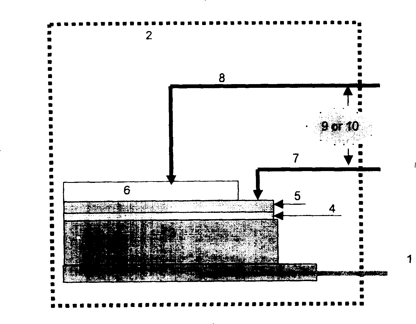
[0035] (1) Use a silicon oxide wafer as the substrate, the thickness of silicon oxide is 1 μm, first use the magnetron sputtering method to deposit the transition layer Ti at room temperature, the thickness is about 20nm, and then sputter the lower electrode material W, the thickness is 100nm left and right, the power is 300W, and the background vacuum is 4×10 -6 torr, sputtering vacuum is 0.10Pa.

[0036] (2) Magnetron sputtering of GeTeSb film with a thickness of 80 nm, a sputtering power of 100 W, and a background vacuum of 3 × 10 -6 torr, the sputtering vacuum is 0.08Pa.

[0037] (3) Put the prepared materials into figure 1 In the closed container shown, according to Figure 4 The temperature is controlled by rising and falling as shown, and can be evacuated, filled with liquid nitrogen or other gas protection as needed. A ...

Embodiment 2

[0039] Example 2: Example 1 (1)-(4) remain unchanged, by rotating and moving the CASCADE RHM-06 probe station. Characterizing the I-V properties of each point of the GeTeSb film on a 4-inch silicon wafer, we can see the uniformity, repeatability and stability of the GeTeSb film.

Embodiment 3

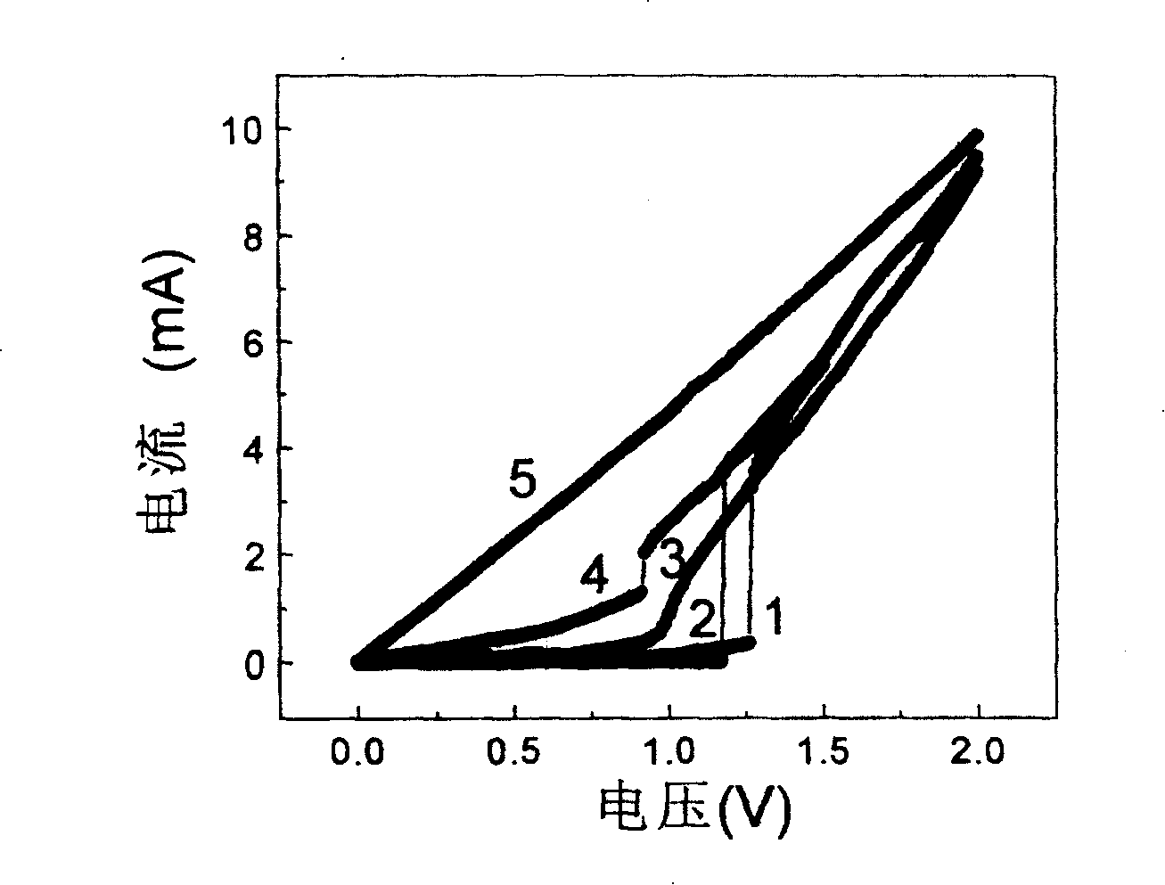
[0040] Example 3: Example 1 (1)-(4) remained unchanged, and the I-V characteristics were studied in a closed heating container at a temperature of 120°C. result with figure 2 resemblance.


PUM

PropertyMeasurementUnit
Diameteraaaaaaaaaa
Thicknessaaaaaaaaaa
Thicknessaaaaaaaaaa

Abstract

The invention relates to a method of electric performance surface features of phase transition material used for praparing phase transition memory. THe characteristics are: to form storage unit by probeg and phase transition material on W / SiO2 / Si substrate, the phase transmition area is occurred at contacted position of needle tip and phase transition material at first, size (vertical and horizontal) of reversible phase transition area is related to needle tip area and electric energy applied on the needle tip, the area of needle tip specify component size of the memory, the transform of phase transition material from amorphous to polycrystal is realized by I-V testing system on interface of the probe, phase transition are can be changed from small to larger until maximum saturation scale by proper voltage and current range and multioperation, it is controlled by pulse height and pulse duration of voltage pulse signal.

Description

technical field [0001] The invention relates to a method for characterizing the electrical properties of reversible phase-change materials, in particular to a simple and practical new method for characterizing the electrical properties of phase-change materials and electrode materials used in the preparation of phase-change memories (PRAM), belonging to microelectronics Preparation process and electrical characterization of nanomaterials in science. technical background [0002] Phase-change random access memory (PRAM, Phase-change-Random Access Memory) technology is based on S.R. Ovshinsky in the late 1960s and early 1970s proposed that the chalcogenide film can be applied to the concept of phase change storage media. A cheap and stable memory device. Due to the limitations of the preparation technology and process at that time, the size of the device was large, the phase change material could only undergo a phase change under a relatively strong electric field, and the st...

Claims


Application Information

Patent Timeline
IPC IPC(8): H01L45/00G11C11/56G11C13/00B82B3/00
Inventor 宋志棠封松林
Owner SHANGHAI INST OF MICROSYSTEM & INFORMATION TECH CHINESE ACAD OF SCI
Why Eureka
Try Eureka