STI channel filling method

A technology of trench filling and trenching, which is applied in electrical components, semiconductor/solid-state device manufacturing, circuits, etc., can solve the problems of reducing the performance of the STI insulating isolation filling layer, aggravating the leakage current of the insulating isolation layer, and improper content ratio, etc., to achieve The effect of increasing the amount, eliminating silicon particles, and increasing the content ratio

Inactive Publication Date: 2008-08-20
SEMICON MFG INT (SHANGHAI) CORP +1
View PDF4 Cites 0 Cited by
  • Summary
  • Abstract
  • Description
  • Claims
  • Application Information

AI Technical Summary

Problems solved by technology

However, if the H during the HDP-CVD process 2 , O 2 and SiH 4 If the content ratio is not appropriate, excess silicon particles will be produced during the deposition process
These excess silicon particles stay in the STI-filled silicon oxide film, which not only causes leakage current, but also causes scratches and voids during the CMP (Chemical Mechanical Polishing) process, further aggravating the leakage current in the insulating isolation layer generation, reducing the performance of the STI insulating isolation filling layer

Method used


Image

  • STI channel filling method
  • STI channel filling method
  • STI channel filling method

Examples


Embodiment Construction

[0033] The specific embodiments of the present invention will be described in detail below in conjunction with the accompanying drawings.

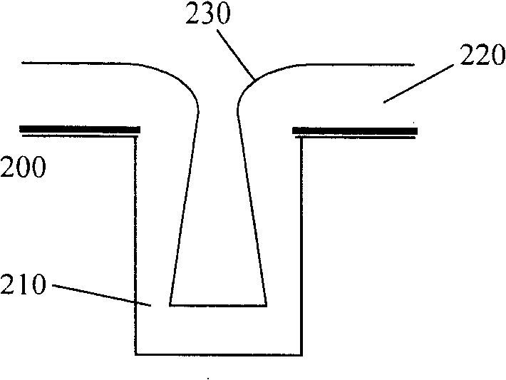
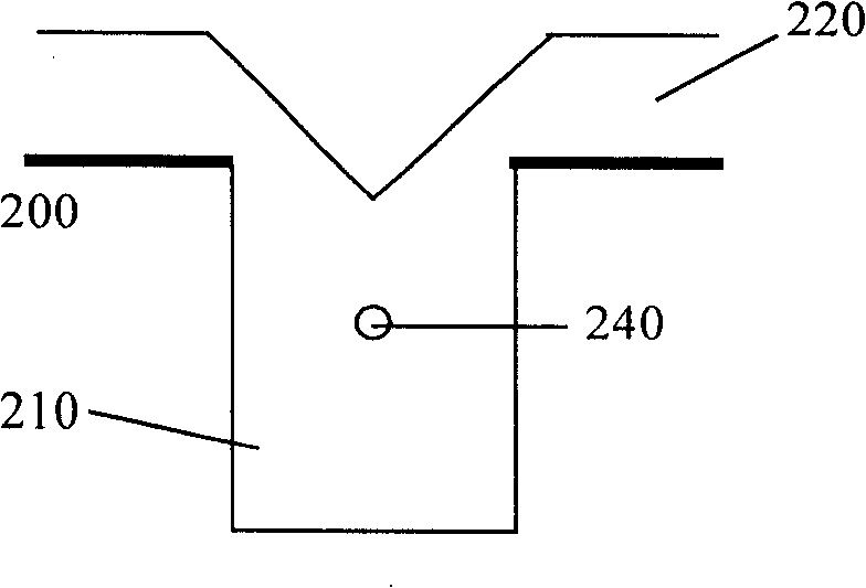
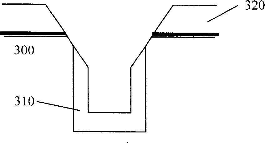
[0034] The STI trench isolation structure is used in integrated circuits as an isolation technology between components. The components are separated by etched trenches to insulate them from each other. The silicon oxide filling method for STI trenches of the present invention firstly provides a substrate in a reaction chamber, and forms trenches on the substrate by using processes such as masking, photolithography and etching. For the shallow trench isolation structure of the semiconductor process below 0.13 μm, the aspect ratio of the trench is generally greater than 3; and for the shallow trench isolation structure of the 90nm semiconductor process, the aspect ratio of the trench is Will reach 4 or higher, and the width is about 130-140nm.

[0035] The function of the STI trench is to isolate and insulate the components between multipl...


PUM


Abstract

The method for filling in STI groove includes steps: forming groove on substrate placed inside reaction chamber in advance; using chemical vapor deposition (CVD) technique including sputtering technique in groove inside chamber to fill silicon oxide; reacting gas utilized including oxygen and silicane for CVD technique as well as hydrogen and helium gases for sputtering technique; continuing to let oxygen into reaction chamber, carrying out plasma process for oxygen, and using oxygen plasma in high density to remove fine particles of silicon residual in silicon oxide. Thus, the invention raises quality of fill film.

Description

technical field [0001] The present invention relates to semiconductor technology, particularly to a kind of trench filling (Gap-filling) silicon oxide (SiO 2 )Methods. Background technique [0002] As the semiconductor technology enters the deep submicron era, components below 0.18 μm, such as the active isolation layer of the MOS circuit, have mostly been fabricated by the Shallow Trench Isolation (STI) process. In this process, shallow trenches are first formed on the substrate, and the elements are separated by etched shallow trenches, and then dielectrics are filled in the shallow trenches by chemical vapor deposition (CVD), such as Silicon oxide, after sidewall oxidation and dielectric filling, the wafer surface is planarized by chemical mechanical polishing (CMP). [0003] Since the aspect ratio AR of the shallow trench of the deep submicron device is relatively high, high-density plasma chemical vapor deposition (High-Density-Plasma CVD, HDP-CVD) is generally used t...

Claims


Application Information

Patent Timeline
Patent Type & Authority Patents(China)
IPC IPC(8): H01L21/762H01L21/316
Inventor 汪钉崇
Owner SEMICON MFG INT (SHANGHAI) CORP
Why Eureka
Try Eureka