A cathode preparing method for improving field emission stability of printed carbon nanotube film
A carbon nanotube film, carbon nanotube technology, applied in cold cathode manufacturing, discharge tube/lamp manufacturing, electrode system manufacturing, etc., to increase contact area, improve field emission stability, improve ohmic contact and thermal conductivity. Effect
- Summary
- Abstract
- Description
- Claims
- Application Information
AI Technical Summary
Problems solved by technology
Method used
Image
Examples
Embodiment 1
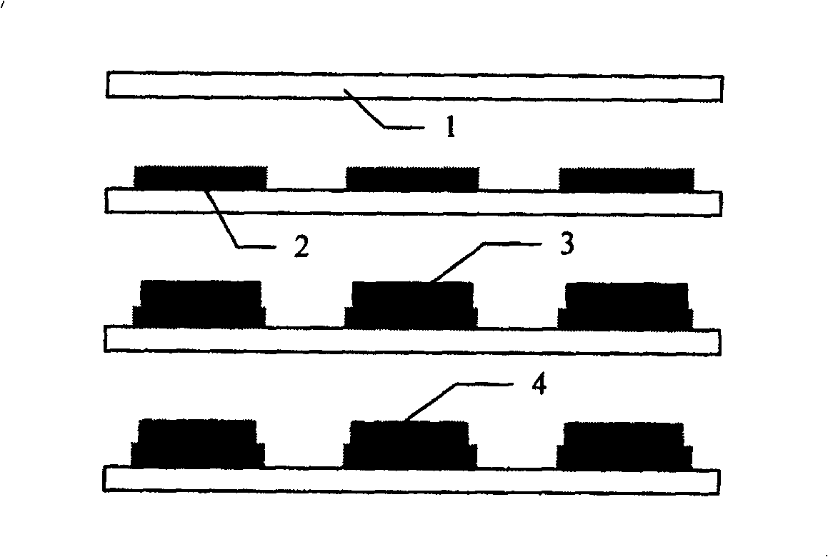
[0024] The first embodiment of the present invention that the inventor provides is to manufacture the monochrome carbon nanotube field emission flat panel display with X-Y addressing of dipole structure, and its manufacturing process is as follows:
[0025] 1. Substrate selection and pretreatment
[0026] In this embodiment, ordinary soda-lime glass is used as the substrate 1 . Use detergent to wash off the oil stains on the glass, then use pure water to clean the detergent, and finally use compressed air to dry the glass for later use.
[0027] 2. Purification of Carbon Nanotubes
[0028] The carbon nanotubes used in this embodiment are multi-walled carbon nanotubes prepared by CVD, which contain a lot of impurities mainly including catalyst particles (mainly iron and its oxides). Purification is mainly to remove these impurities. Since the catalyst used in the preparation of carbon nanotubes will exist in carbon nanotubes, it should be removed during use. The carbon nanot...
Embodiment 2
[0049] The second embodiment of the present invention that the inventor provides is to manufacture the color carbon nanotube field emission flat panel display with X-Y addressing of the dipole structure, and its preparation process is exactly the same as embodiment 1, and the difference is that in the anode plate In the manufacturing step 7, the phosphor powders are three colors, and the phosphor powders of the three colors are printed separately. A color carbon nanotube field emission flat panel display with X-Y addressing can be obtained.
Embodiment 3
[0051] The third embodiment of the present invention that the inventor provides is to manufacture the electron source of high-power microwave device, and its manufacturing process is as follows:
[0052] 1. Substrate production
[0053] According to the design requirements and selecting the appropriate material to make the conductive base of appropriate shape. For example, stainless steel or graphite materials are processed into disc-shaped cathode substrates with circular joints (the joints are used to connect with the device and are located at the bottom of the disc), and then the surface is ground and cleaned before entering other Production process;
[0054] 2. Other production processes
[0055] Other manufacturing processes are the same as steps 2-6 in Example 1. The electron source of the high power microwave device can be obtained.
PUM
 Abstract
Description
Claims
Application Information
