Method for finishing hard mask layer, method for forming transistor grids, and stack structure

A technology of hard mask layer and stacked structure, which is applied in the direction of semiconductor devices, semiconductor/solid-state device manufacturing, electrical components, etc., and can solve the problem of poor gate structure, distorted pattern of hard mask layer 108, damage to process flow and results, etc. question

Active Publication Date: 2009-08-12
UNITED MICROELECTRONICS CORP
View PDF2 Cites 0 Cited by
  • Summary
  • Abstract
  • Description
  • Claims
  • Application Information

AI Technical Summary

Problems solved by technology

[0008] However, since the antireflection bottom layer 110 is etched by carbon tetrafluoride and trifluoromethane faster than the hard mask layer 108, this method often causes the hard mask layer 108 to be etched near the antireflection bottom layer 110. greater than the portion near the conductive layer 106, the hard mask layer 108 thus becomes a distorted pattern
Therefore, under the condition that the hard mask layer 108 has been deformed, it is used as an etching mask for etching the conductive layer 106 to form a gate, and the gate structure produced by it is not good.
More importantly, the anti-reflective bottom layer 110 is prone to photoresist line collapse (line collapse) during the trimming process and subsequent etching of the conductive layer, which will seriously damage the entire process flow and results.

Method used


Image

  • Method for finishing hard mask layer, method for forming transistor grids, and stack structure
  • Method for finishing hard mask layer, method for forming transistor grids, and stack structure
  • Method for finishing hard mask layer, method for forming transistor grids, and stack structure

Examples


Embodiment Construction

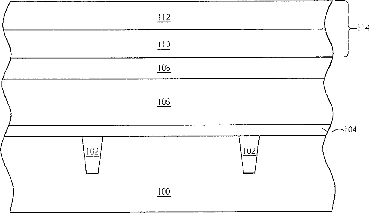
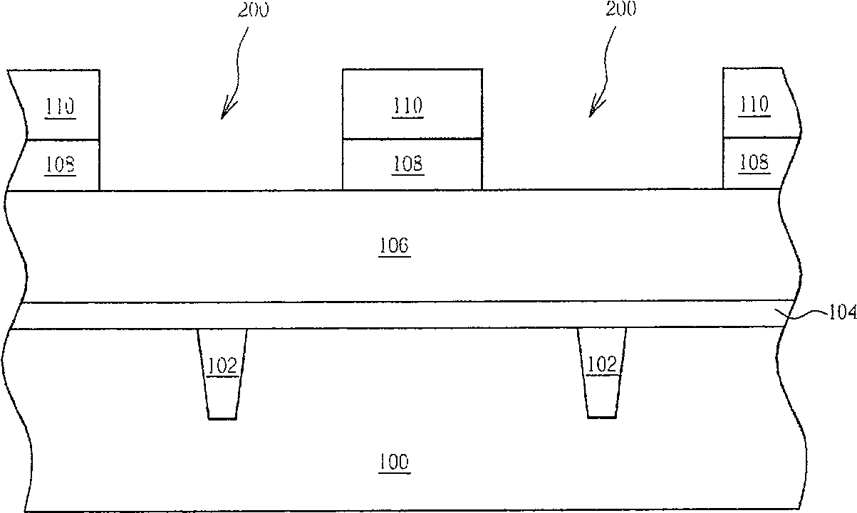
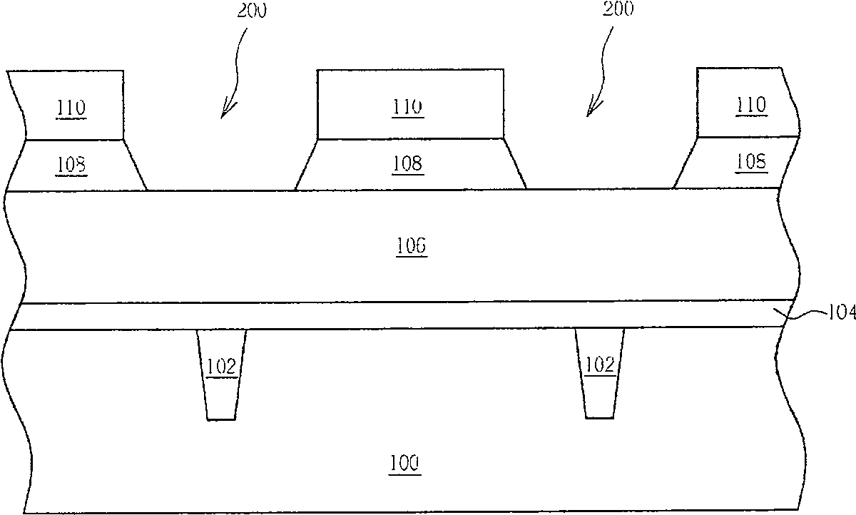
[0038] Please refer to Figure 4 to Figure 10 . Figure 4 to Figure 10 It is a schematic diagram of the process of forming the gate of the metal oxide semiconductor transistor according to the present invention. Please refer to Figure 4 , providing a substrate 400, generally made of single crystal silicon, or silicon on insulation (SOI), or other semiconductor materials that can be used in this technology, such as: strained silicon (strained silicon), strained insulating layer Strained silicon-on-insulator, silicon-germanium, strained silicon-germanium, silicon-germanium on insulator, germanium, strained germanium ( strained germanium), germanium oninsulator (GeOI), strained germanium on insulator, strained semiconductor, compound semiconductor, compound semiconductor and Multilayer semiconductor (multi-layerssemiconductor) instead.

[0039] Substrate 400 includes several silicon dioxide (SiO 2 ) or a low-k dielectric material such as a shallow trench isolation (shallow ...


PUM


Abstract

A method for trimming a hard mask layer provides a substrate, a hard mask layer, and a three-layer stack layer on the substrate. The three-layer stack includes a top photoresist, a silicon-containing layer, and a bottom photoresist. The top photoresist, the silicon-containing layer, the bottom photoresist and the hard mask layer are sequentially patterned, and then a trimming process is performed on the hard mask layer. Since the underlying photoresist of the present invention is thin and is worn out during etching, photoresist line collapse does not occur.

Description

technical field [0001] The invention relates to a method for trimming a hard mask layer, in particular to a method for improving the trimming of the hard mask layer by using three photoresist layers to form a gate of a metal oxide semiconductor transistor. Background technique [0002] As semiconductor manufacturing technology becomes more and more sophisticated, integrated circuits have undergone major changes, which has led to a rapid increase in computing performance and storage capacity of computers, and has driven the rapid development of peripheral industries. The semiconductor industry is also developing at the speed of doubling the number of transistors on integrated circuits every 18 months, as predicted by Moore's Law. 90 nanometers (nm) (0.09 microns), entering 65 nanometers (0.065 microns process) in 2005 and moving towards 45 nanometers. [0003] In the process of fabricating a metal oxide semiconductor transistor (MOS transistor), forming a conductive gate is ...

Claims


Application Information

Patent Timeline
Patent Type & Authority Patents(China)
IPC IPC(8): H01L21/027H01L21/033H01L21/31H01L21/28H01L21/3213
Inventor 王明俊陈薏新杨闵杰廖俊雄
Owner UNITED MICROELECTRONICS CORP
Why Eureka
Try Eureka