A ballasting resistor structure of microwave power transistor dynamic emitter electrode

A microwave power and ballast resistance technology, which is applied in the manufacture of transistors, semiconductor/solid-state devices, circuits, etc., can solve the problems of insufficient thermal coupling of ballast resistance, loss of microwave power gain of devices, and limiting additional ballast effect. Meet the requirements of microwave performance and reliability, reduce parasitic capacitance and chip area, and increase the effect of additional ballast effects

Inactive Publication Date: 2009-08-26
NO 55 INST CHINA ELECTRONIC SCI & TECHNOLOGYGROUP CO LTD
View PDF4 Cites 1 Cited by
  • Summary
  • Abstract
  • Description
  • Claims
  • Application Information

AI Technical Summary

Problems solved by technology

However, the existence of the emitter ballast resistor will reduce the microwave power gain of the transistor; at the same time, the PN junction of the diffusion resistor will increase the parasitic capacitance from the collector to the emitter, which is detrimental to the stability of the device.
[0005] Existing diffused emitter ballast resistors are generally designed on the edge of one side of the active area of ​​the chip, and the thermal coupling of the active area to the ballast resistor is insufficient, which limits the additional ballast effect. At the same time, the existence of the ballast resistor increases the collector to The parasitic capacitance between the emitter
When designing multiple active areas, a ballast resistor must be designed for each active area, which increases the parasitic capacitance of the ballast resistor and the chip area. The existence of the emitter ballast resistor is beneficial to the reliability of the device, but it is harmful to the microwave Loss of power gain

Method used


Image

  • A ballasting resistor structure of microwave power transistor dynamic emitter electrode
  • A ballasting resistor structure of microwave power transistor dynamic emitter electrode
  • A ballasting resistor structure of microwave power transistor dynamic emitter electrode

Examples


Embodiment Construction

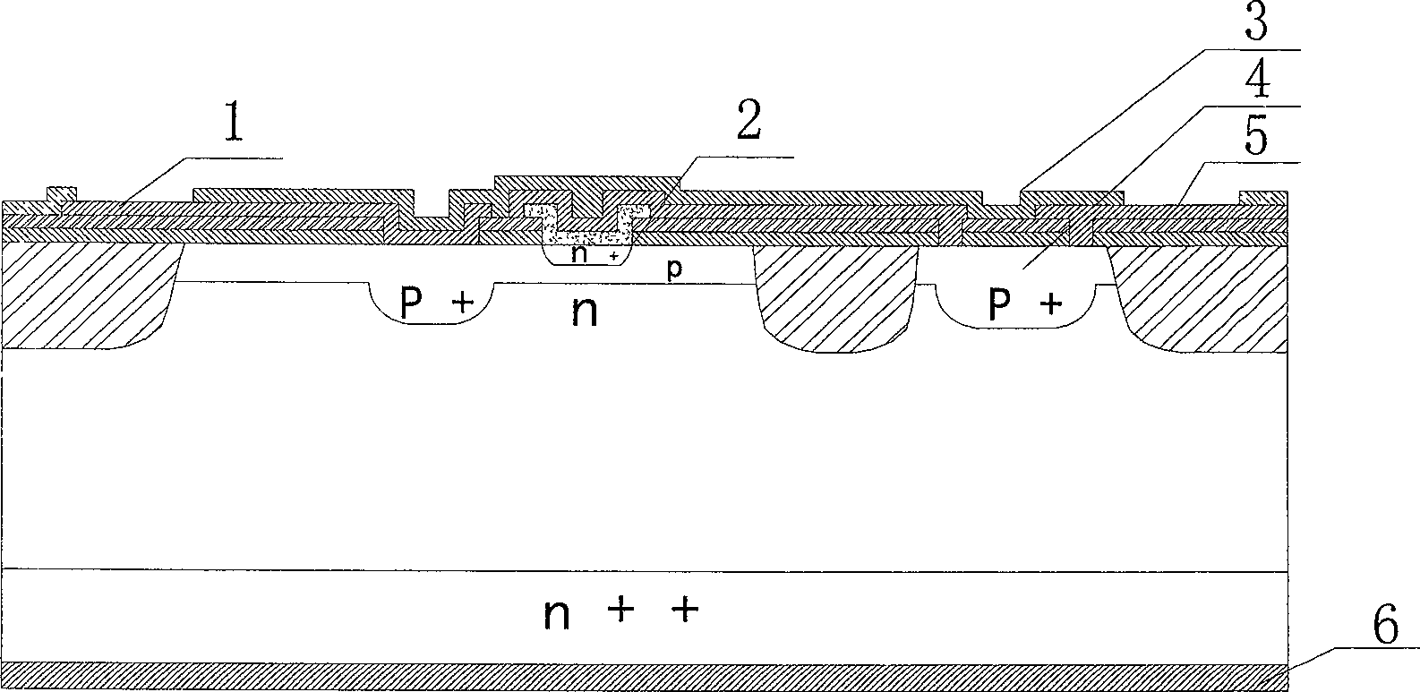
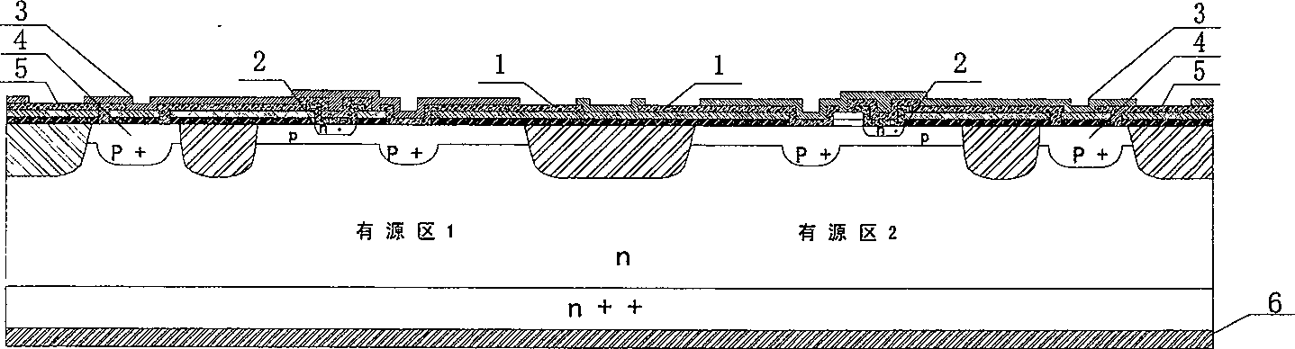
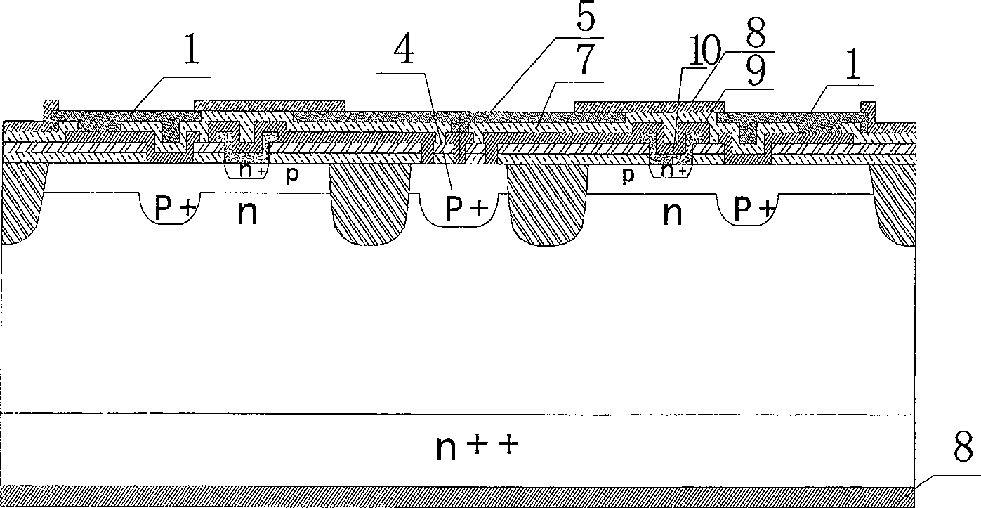
[0059] 1 in the figure is the base metal bonding region; 2 is the n+ doped emitter region, and the emitter region and its corresponding p-type base region and n-type collector region together form the active region; 3 is the passivation dielectric film on the metal surface; 4 is the P+ doped emitter ballast resistance area, with a thickness of 1μm-2μm; 5 is the emitter metal bonding area; 6 is the collector; n ++ for the silicon substrate. The thickness of p region is 0.3μm-0.4μm; n + The thickness of the region is 0.1μm-0.2μm; the thickness of the n-type silicon epitaxial layer is 3μm-14μm; n ++ The thickness of the silicon substrate material is 380 μm-560 μm. 7 is an isolation dielectric film between double-layer metals; 8 is a passivation layer on the metal surface. 9 is the interconnection metal of the emitter window and the ballast resistor window; 10 is n + launch area, n + The emitter region and its corresponding p-type base region and n-type collector region toget...


PUM


Abstract

The present invention is a dynamic emitter ballast resistor structure of a microwave power transistor. The structure is that the active area is divided into two adjacent areas, the emitter ballast resistor is placed between the two active areas, and the emitter and base electrodes adopt double The layer metal wiring leads out, and the two active areas share a ballast resistor. Advantages: The active area is divided into two adjacent areas, the emitter ballast resistor is placed between the two active areas, and the emitter and base electrodes are drawn out by double-layer metal wiring. Make the two active regions fully thermally coupled to the same ballast resistance, make the ballast resistance value increase with the increase of temperature, increase the additional ballast effect, and realize dynamic ballast. Share a ballast resistor, reduce the parasitic capacitance of the ballast resistor and the chip area. Increase the heat dissipation boundary of the active area and reduce the thermal resistance. For chips with the same power and ballast resistance, the peak junction temperature drops by 15°C-20°C. Meet the requirements of microwave power transistors for microwave performance and reliability.

Description

technical field [0001] The invention relates to a dynamic emitter ballast resistor structure and production method of a microwave power transistor, belonging to the technical field of semiconductor microelectronic design and manufacture. Background technique [0002] The focus and difficulty in the design and manufacture of microwave power transistors mainly include the following three aspects: 1. To overcome the adverse effects of microwave parasitic parameters and improve microwave gain performance. 2. Overcome the large injection effect in the base area, improve the power capacity, and maintain the microwave performance under high-power conditions; 3. Overcome the thermal effect brought by high-power applications, and improve the long-term reliability of the transistor. [0003] Microwave power devices often work under high power density conditions, and their efficiency is low at high frequencies, which increases dissipation and produces high junction temperatures. Even ...

Claims


Application Information

Patent Timeline
Patent Type & Authority Patents(China)
IPC IPC(8): H01L29/73H01L21/331
Inventor 傅义珠
Owner NO 55 INST CHINA ELECTRONIC SCI & TECHNOLOGYGROUP CO LTD
Why Eureka
Try Eureka