Grids and method of manufacture

A manufacturing method and gate technology, applied in semiconductor/solid-state device manufacturing, electrical components, semiconductor devices, etc., can solve problems such as the inability to accurately control the line width at the bottom of the gate, and achieve the limitation of lithography resolution and reliability High and stable electrical parameters

Inactive Publication Date: 2009-09-09
SEMICON MFG INT (SHANGHAI) CORP +1
View PDF4 Cites 0 Cited by
  • Summary
  • Abstract
  • Description
  • Claims
  • Application Information

AI Technical Summary

Problems solved by technology

[0009] Therefore, the object of the present invention is to provide a gate and its manufacturing method to solve the problem that the bottom line width of the formed gate cannot be accurately controlled in the existing gate manufacturing method

Method used


Image

  • Grids and method of manufacture
  • Grids and method of manufacture
  • Grids and method of manufacture

Examples


Embodiment Construction

[0024] In order to make the above objects, features and advantages of the present invention more comprehensible, specific implementations of the present invention will be described in detail below in conjunction with the accompanying drawings.

[0025] Figure 7 It is a flow chart of an embodiment of the method for forming a gate with a groove at the bottom of the present invention.

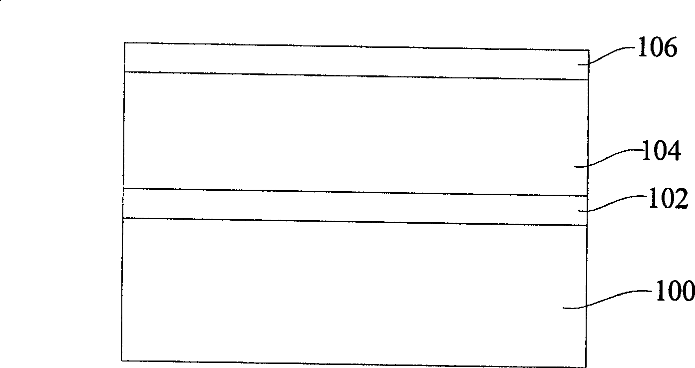
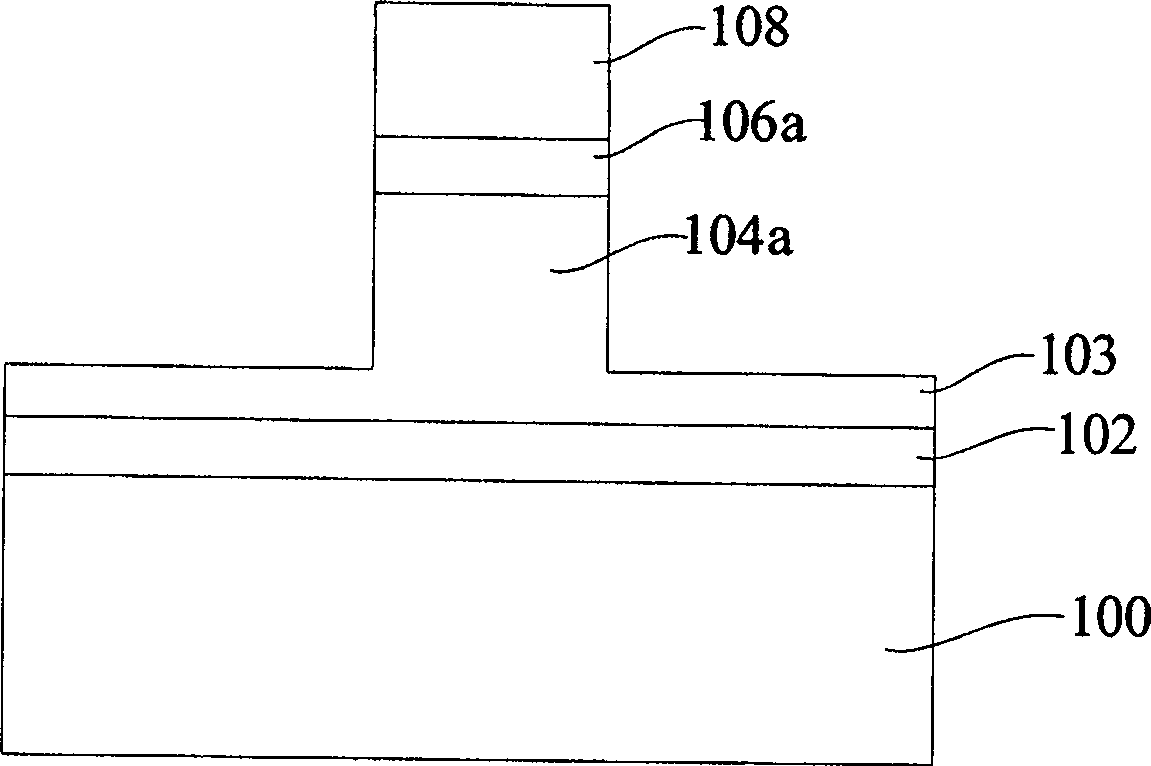
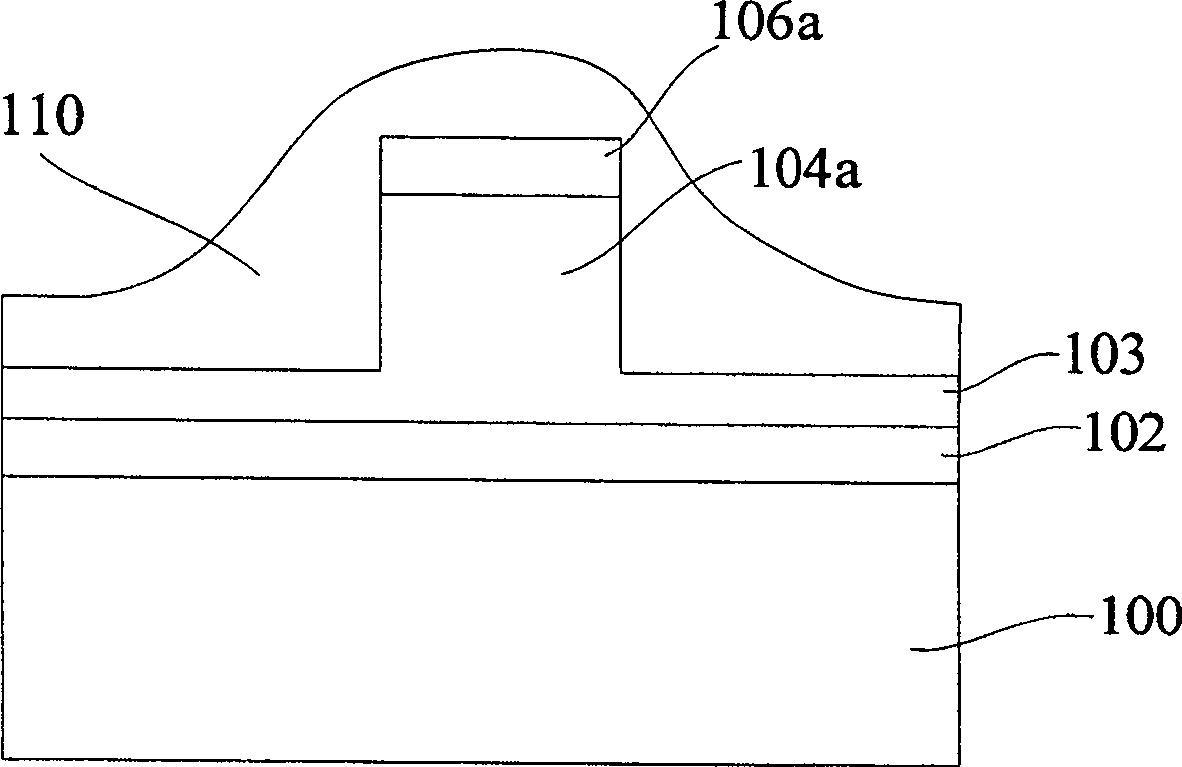
[0026] like Figure 7 As shown, firstly, a semiconductor substrate is provided ( S100 ). The semiconductor base is one of polysilicon, single crystal silicon, amorphous silicon, silicon on insulating layer, silicon germanium composition and gallium arsenide. Doping N-type impurities or P-type impurities into the semiconductor substrate to form a conductive channel of the device. The surface of the semiconductor substrate has a thin oxide layer, the thickness of the oxide layer is 1 to 100 nm, and the formation method of the oxide layer is high temperature thermal oxidation or deposition. The ...


PUM

PropertyMeasurementUnit
thicknessaaaaaaaaaa
thicknessaaaaaaaaaa

Abstract

A method for manufacturing a gate, comprising: providing a semiconductor substrate; forming a first dielectric layer on the semiconductor substrate; forming at least a second dielectric layer on the first dielectric layer; Forming a groove in the second dielectric layer, the bottom of the groove exposes the substrate surface; removing the second dielectric layer; forming a conductive layer in the groove of the first dielectric layer and on the first dielectric layer layer; spin-coat a photoresist layer on the conductive layer and pattern it to form a gate pattern, and the gate pattern is located above the groove of the first dielectric layer; The conductive layer and the first dielectric layer covered by the pole pattern. This method can more accurately control the line width of the bottom of the formed gate.

Description

technical field [0001] The invention relates to the technical field of semiconductor manufacturing, in particular to a gate (notched gate) with a groove at the bottom and a manufacturing method thereof. Background technique [0002] With the development of the semiconductor manufacturing process, the integration of semiconductor devices is getting higher and higher, and the size is getting smaller and smaller, which requires the line width in the semiconductor manufacturing process to be made smaller and smaller. Usually, the size of the gate in a semiconductor device represents the process level of the semiconductor device manufacturing process. Reducing the gate of a semiconductor device first requires improving the resolution of the photolithography process, such as using a short-wavelength light source and advanced mask correction technology. But this requires a lot of economic and time costs. An existing method for reducing the line width of the gate is to form a groov...

Claims


Application Information

Patent Timeline
Patent Type & Authority Patents(China)
IPC IPC(8): H01L21/28H01L21/336H01L29/78H01L29/423
Inventor 张海洋陈海华黄怡马擎天
Owner SEMICON MFG INT (SHANGHAI) CORP
Why Eureka
Try Eureka