
Method for assembling semiconductor chips, and corresponding semiconductor chip assembly

A semiconductor and chip technology, applied in the field of semiconductor chip devices, can solve problems such as increased cost, and achieve the effects of favorable energy efficiency, high K coefficient, and high mechanical strength

Inactive Publication Date: 2010-01-27
ROBERT BOSCH GMBH
View PDF7 Cites 0 Cited by
  • Summary
  • Abstract
  • Description
  • Claims
  • Application Information

AI Technical Summary

Problems solved by technology

[0019] In this example, the basis for Figure 7 Or 8 glass stems 140,140 ', they cause the increase of cost when manufacturing, because the sensor chip 5 ' of surface micromachine

Method used


Image

  • Method for assembling semiconductor chips, and corresponding semiconductor chip assembly
  • Method for assembling semiconductor chips, and corresponding semiconductor chip assembly
  • Method for assembling semiconductor chips, and corresponding semiconductor chip assembly

Examples


Embodiment Construction

[0052] The same reference numerals in the drawings indicate the same or functionally identical components.

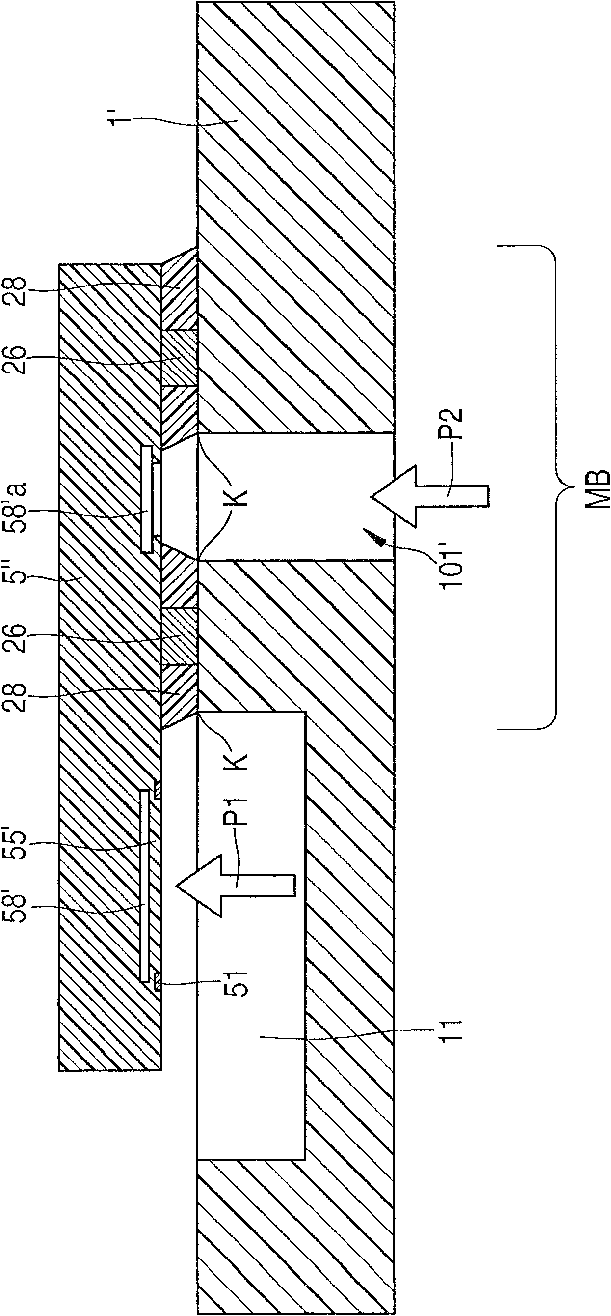
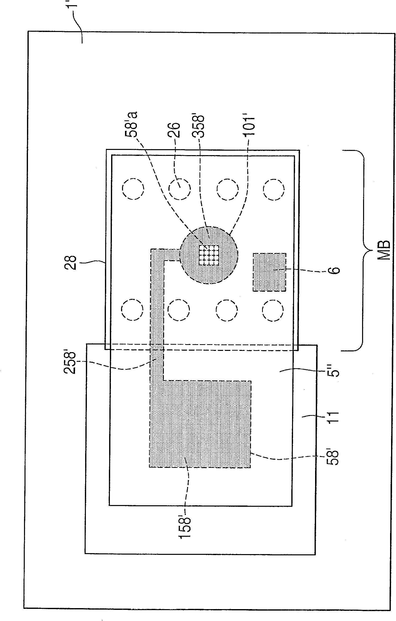
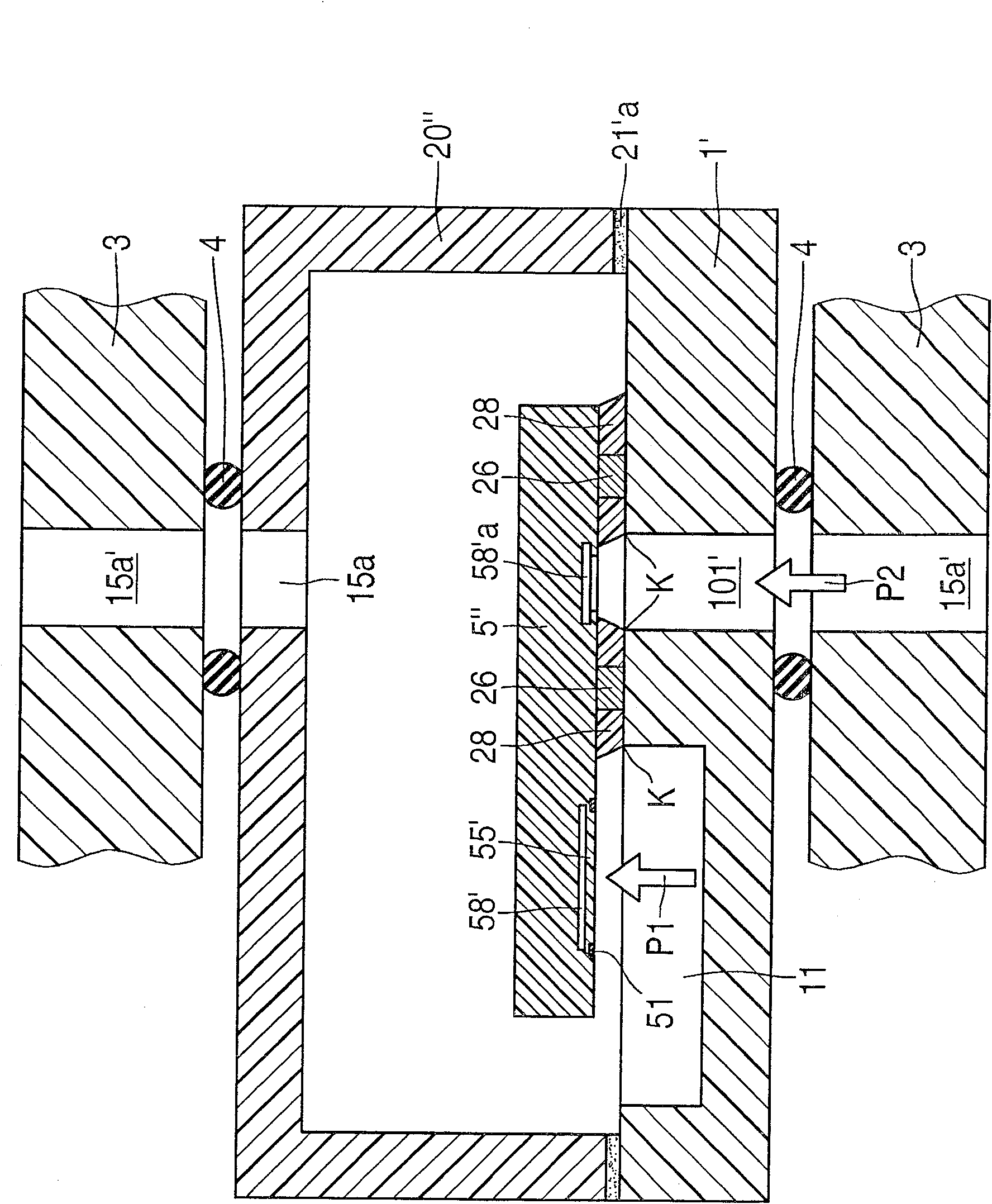
[0053] Figure 1a , b represents a lateral and horizontal cross-section of a first embodiment of the method for mounting semiconductor chips and the corresponding semiconductor device according to the invention.

[0054] In this example the sensor chip 5 ″ is a surface micromechanical sensor chip which is produced, for example, according to the method described in DE 100 32 579 A1 and which has a cavity 58 ′ combined on a membrane region 55 ′.

[0055] For assembly, the bonding pads of the sensor chip 5 ″ are soldered to the (not shown) bonding pads of the substrate 1 ′ in a mounting region MB by means of a solder or adhesive connection, for example by means of a solder bead 26 , here the substrate is a printed circuit board or ceramic and has a recess 11 next to which the sensor chip 5 ″ is mounted suspended in flip-chip technology.

[0056] The assembly area MB also...


PUM


Abstract

The invention relates to a method for assembling semiconductor chips, comprising the following steps: a semiconductor chip (5'') is provided that has a surface encompassing a membrane area (55') and a peripheral area. The peripheral area is provided with an assembly area (MB) while a cavity (58') that extends all the way to the assembly area (MB) and joins an opening (58'a) there is located below the membrane area (55'); a substrate (1'; 10) is provided which has a surface with a recess (11); the assembly area (MB) of the semiconductor chip (5'') is assembled on the surface of the substrate (1'; 10) by means of a flip-chip technique in such a way that an edge (K) of the recess (11) lies between the assembly area (MB) and the membrane area (55') while the opening (58'a) is oriented towards the substrate (1'; 10); the assembly area (MB) is filled underneath with a filling (28), the edge (K) of the recess (11) being used as a break-off area for the filling (28) such that no filling (28) penetrates into the membrane area (55); and a continuous hole (101'; 101'') is provided through the substrate (1'; 10) to the opening (58'a) of the cavity (58'). The invention also relates to a corresponding semiconductor chip assembly.

Description

technical field [0001] The invention relates to a method for mounting semiconductor chips and a corresponding semiconductor chip arrangement. [0002] Although the invention can be applied to any desired semiconductor chip arrangement, the invention and the problem on which it is based will only be described with reference to a micromechanical semiconductor chip arrangement with a pressure sensor. Background technique [0003] Various examples of methods for mounting semiconductor chips and corresponding semiconductor devices are known from DE 102 004 011 203, three of which will be described in detail below. [0004] Figure 7 A cross-section of a first example of a method for mounting a semiconductor chip and a corresponding semiconductor device is shown. [0005] Figure 7 Reference numeral 100 denotes a TO8 socket made of Kovar alloy, for example. Reference numeral 5 is a micromechanical silicon pressure sensor chip with piezoresistive transducer elements 51 which are ...

Claims


Application Information

Patent Timeline
Patent Type & Authority Patents(China)
IPC IPC(8): B81B7/00G01L9/00
CPCG01L19/147G01L19/141G01L9/0054G01L19/0636H01L2924/10253H01L2224/48472H01L2224/48091G01L19/0038H01L2224/8592H01L2924/15151H01L2924/16151H01L2924/16152H01L2924/00014H01L2924/00
Inventor 胡贝特·本泽尔
Owner ROBERT BOSCH GMBH
Learn More