Stacked wafer for 3-D integration

A technology of stacking wafers and wafers, which is applied in the manufacture of electrical components, electrical solid-state devices, semiconductor/solid-state devices, etc., and can solve problems such as complex connections

Inactive Publication Date: 2007-07-18
TEZZARON SEMICON S PTE
View PDF5 Cites 27 Cited by
  • Summary
  • Abstract
  • Description
  • Claims
  • Application Information

AI Technical Summary

Problems solved by technology

In any case, the fabrication of such stacked devices involves a considerable level of fabrication cost, as the connectivity between the devices requires more complex connections in order to obtain the desired results

Method used


Image

  • Stacked wafer for 3-D integration
  • Stacked wafer for 3-D integration
  • Stacked wafer for 3-D integration

Examples


Embodiment Construction

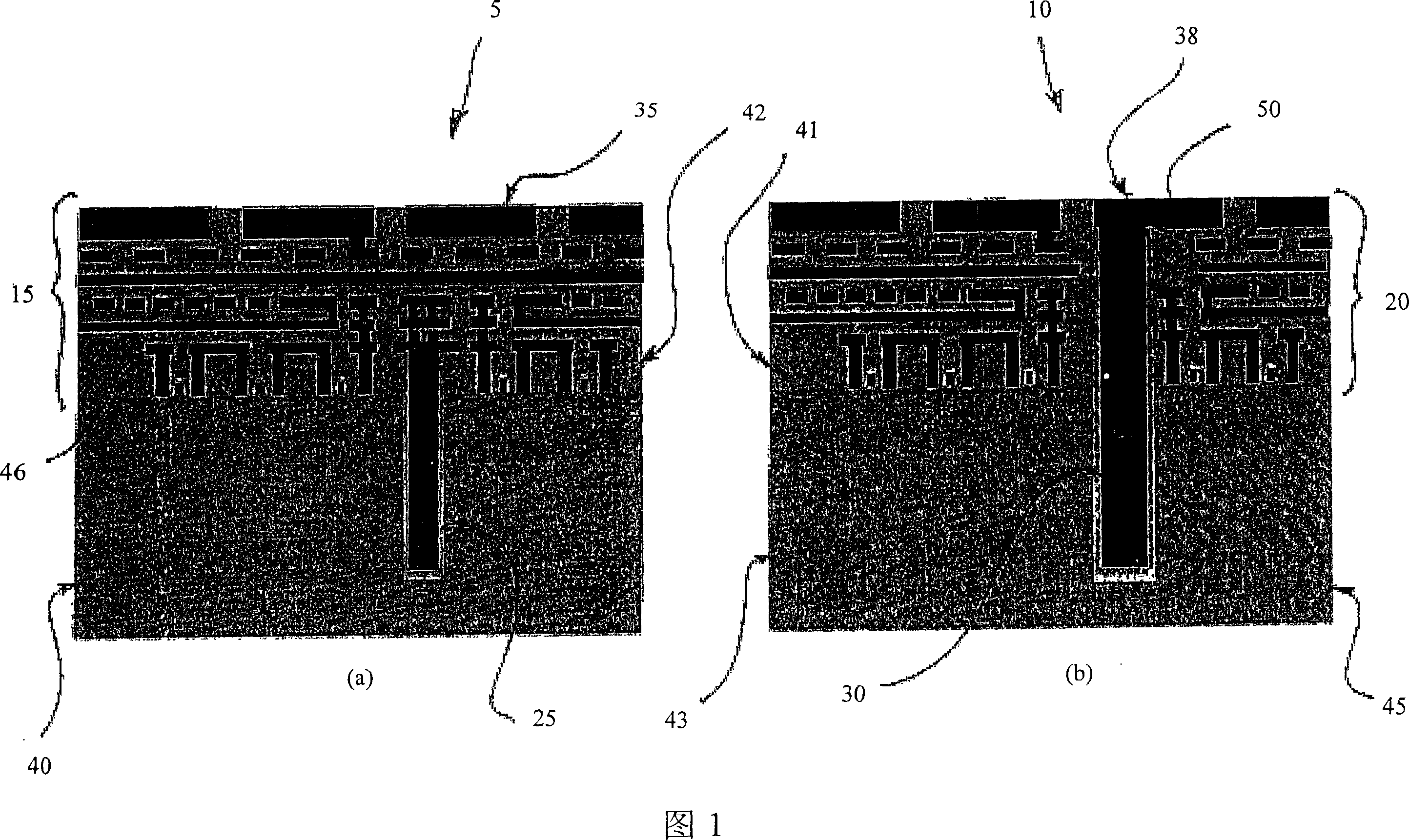
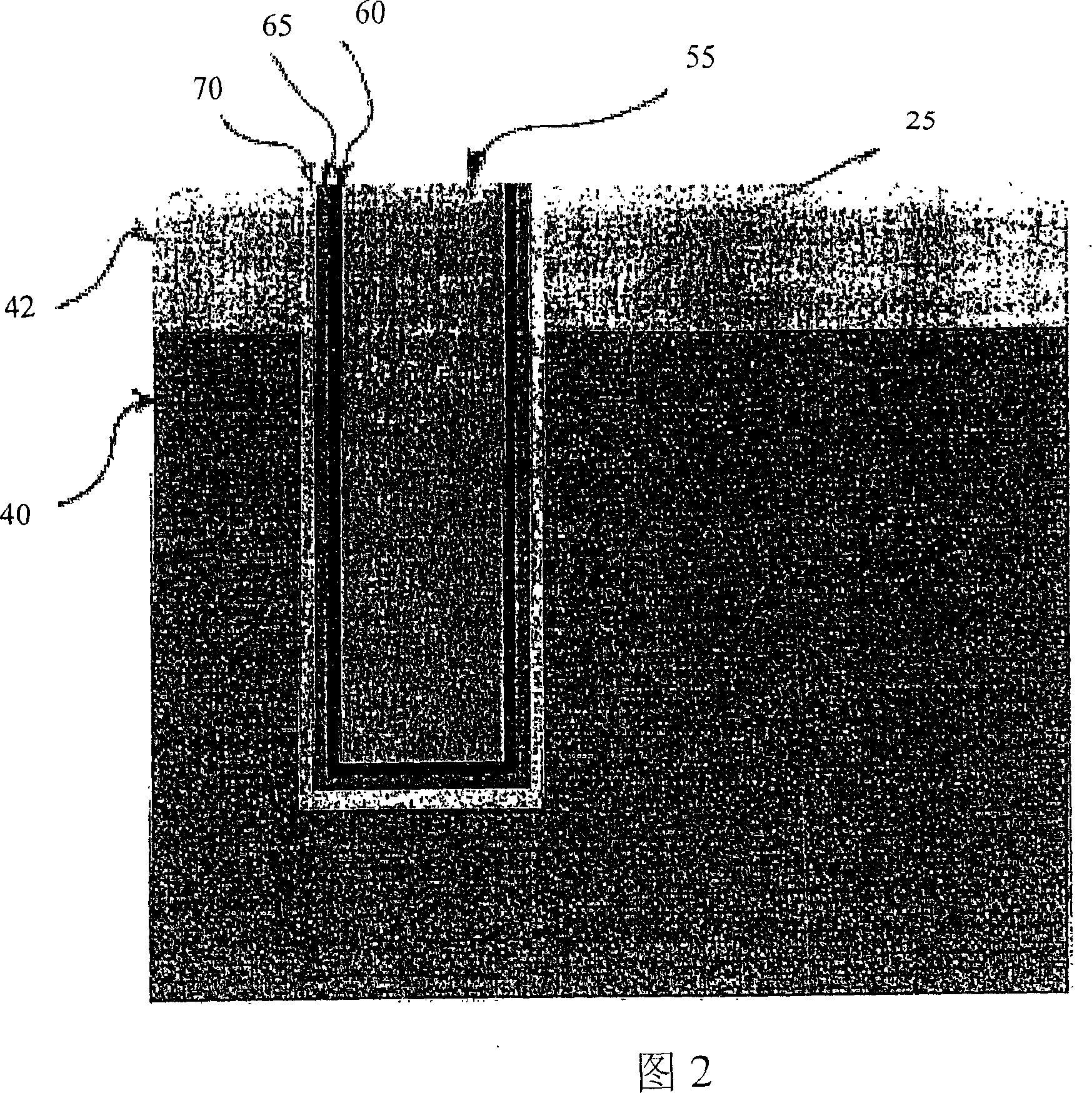
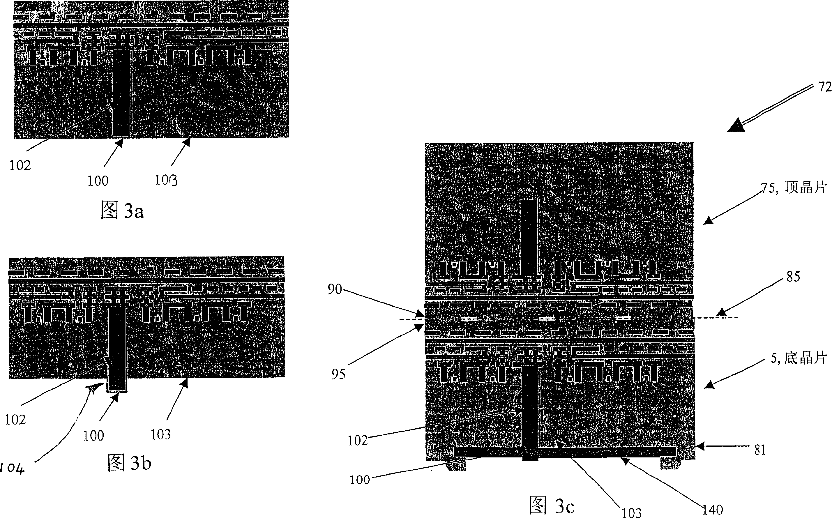
[0048] Figures 1a and 1b show two embodiments of the invention both comprising IC layered CMOS process wafers. IC layers 15 , 20 have been formed in dielectric layers 41 , 42 and together on silicon substrates 40 , 45 . The outer surface of the wafer 5, 10 has copper pads 35, 38 embedded in the surface of the dielectric.

[0049] The main point of difference between the embodiments of FIGS. 1 a and 1 b is the arrangement of the vertical connectors 25 , 30 . In the case of FIG. 1a, the vertical connectors have been embedded in the wafer 5 before the formation of the first IC layer 46 (Metal-1). Figure 1 b has the vertical connector 30 embedded in the wafer 10 after the integrated circuit layer 20 is placed, but before the copper pads 38 are placed. In fact, the present invention is not dependent on any particular location or stage of formation of the vertical connectors 25, 30, which may be placed before any IC metal layers (eg, Metal-1 through Metal-6 of FIG. 1).

[0050] T...


PUM

PropertyMeasurementUnit
diameteraaaaaaaaaa
thicknessaaaaaaaaaa
thicknessaaaaaaaaaa

Abstract

The invention discloses a method for producing a stack wafer device, including the steps: providing a first wafer; forming a plurality of brazing trays on the first surface of the first wafer; forming at least an embedded vertical linker separated from the brazing trays of the first wafer in the first wafer; providing a second wafer; forming a plurality of brazing trays on the first surface of the second wafer, the posithion of which is coincident to the position of the the brazing trays of the first wafer; forming at least an embedded vertical linker separated from the brazing trays of the second wafer in the second wafer; contacting with the first surface of the wafers in order to contact with the brazing trays; supplying the power to the wafer in the predeterminded pressure and at the predetermined temperature until the brazing trays can be bonded, and the first wafer and the second safer are bonded to produce a stack wafer device.

Description

technical field [0001] The present invention relates to stacked die for integrating multiple die platforms into a single scaled package. In particular, the invention relates to a method for manufacturing said package in order to combine several components in a single integrated structure. Background technique [0002] For many years the semiconductor industry has sought a viable solution to wafer-level integration because it allows distribution and recombination of IC designs on a single substrate using a large number of very short vertical interconnects. The resulting ICs offer higher density and speed due to smaller die size and correspondingly shorter RC delays. Incompatible processes, such as analog and digital (without compromising functionality), can be fabricated on different wafers using a fully optimal process and then recombined to produce a 3-dimensional (3D) IC. Thus, wafer-level heterogeneous substrate integration (eg Si and SiGe for digital and RF components,...

Claims


Application Information

Patent Timeline
Patent Type & Authority Applications(China)
IPC IPC(8): H01L21/603H01L21/98
CPCH01L2224/94
Inventor 洪湘基C·拉马萨米S·古他
Owner TEZZARON SEMICON S PTE
Why Eureka
Try Eureka