Circuit board for reducing electromagnetic interference of electronic product
A technology for electromagnetic interference and electronic products, applied in the direction of printed circuits, electrical components, magnetic/electric field shielding connected to non-printed electrical components, etc., can solve problems such as poor performance, waste of cost and time, etc.
- Summary
- Abstract
- Description
- Claims
- Application Information
AI Technical Summary
Problems solved by technology
Method used
Image
Examples
Embodiment Construction
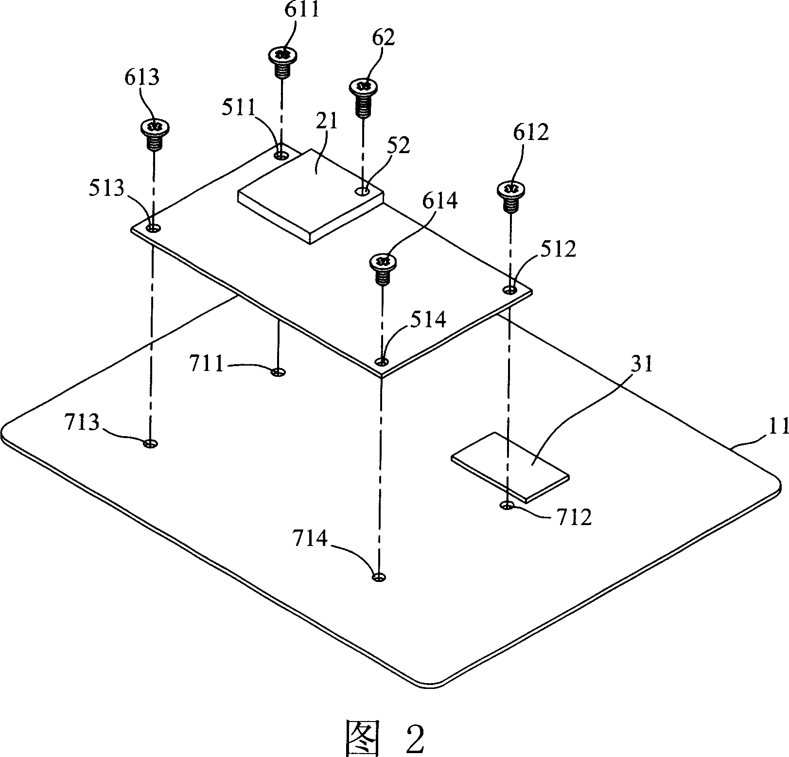
[0017] Please refer to FIG. 2 , which is a circuit block diagram of removing the original ground wire layout and replacing the original transmission wire ground wire layout with metal sheets and screws.
[0018] The printed circuit board 11 includes: a power supply 21 , a load impedance 31 , a metal sheet 41 , a via 711 , a via 712 , a via 713 and a via 714 . The metal sheet 41 has a hole 511 , a hole 512 , a hole 513 and a hole 514 outside the four corners of the metal sheet 41 , and a hole 52 is located on the metal sheet 41 .
[0019] The power supply 21 is a signal source of an AC signal, providing signal sources required by general electronic components. The signal is a voltage or current signal with frequency. The positive pole of the power supply 21 is connected to the load impedance 31 in series through the wiring (trace) on the printed circuit board 11 , while the negative pole of the power supply 21 does not use the wiring method of the printed circuit, but uses a s...
PUM
 Abstract
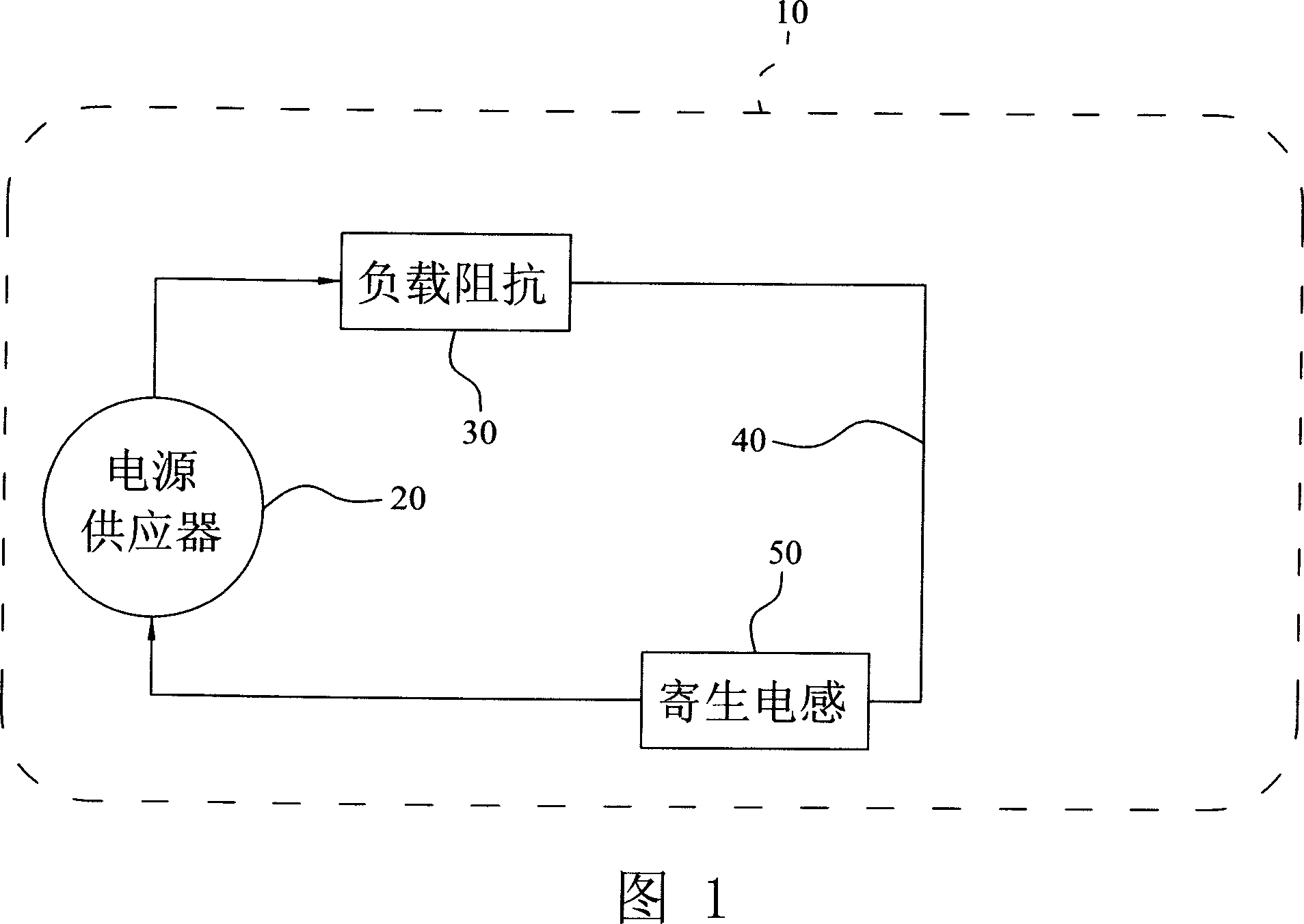
Description
Claims
Application Information
 - R&D
- Intellectual Property
- Life Sciences
- Materials
- Tech Scout
- Unparalleled Data Quality
- Higher Quality Content
- 60% Fewer Hallucinations
Browse by: Latest US Patents, China's latest patents, Technical Efficacy Thesaurus, Application Domain, Technology Topic, Popular Technical Reports.
© 2025 PatSnap. All rights reserved.Legal|Privacy policy|Modern Slavery Act Transparency Statement|Sitemap|About US| Contact US: help@patsnap.com


