Lighting apparatus, exposure apparatus and micro device manufacturing method

A lighting device and exposure device technology, which is applied in the direction of photolithographic process exposure device, optical element, semiconductor/solid-state device manufacturing, etc., can solve the mutual interference between the concentrator optical system 211 and the wafer 214, and increase the concentrator optical system Focal length, improving EUV light reflectivity and other issues, to achieve the effect of preventing light loss, preventing reduction in resolution or contrast, and excellent performance

Inactive Publication Date: 2007-07-25
NIKON CORP
View PDF3 Cites 4 Cited by
  • Summary
  • Abstract
  • Description
  • Claims
  • Application Information

AI Technical Summary

Problems solved by technology

However, the wafer 214 will move in the scanning direction during exposure, so when the condenser optical system 211 is arranged below the position of the wafer 214, the condenser optical system 211 and the wafer 214 will interfere with each other.
Therefore, in the exposure apparatus disclosed in the prior art, it is difficult to increase the reflectivity of EUV light, increase the focal length of the condenser optical system 211, and enlarge the distance between the incident-side fly mirror surface 207 and the exit-side fly mirror surface 208, In this way, the EUV light is incident at an angle close to the reflection surface of the incident-side fly mirror surface 207

Method used


Image

  • Lighting apparatus, exposure apparatus and micro device manufacturing method
  • Lighting apparatus, exposure apparatus and micro device manufacturing method
  • Lighting apparatus, exposure apparatus and micro device manufacturing method

Examples


Embodiment

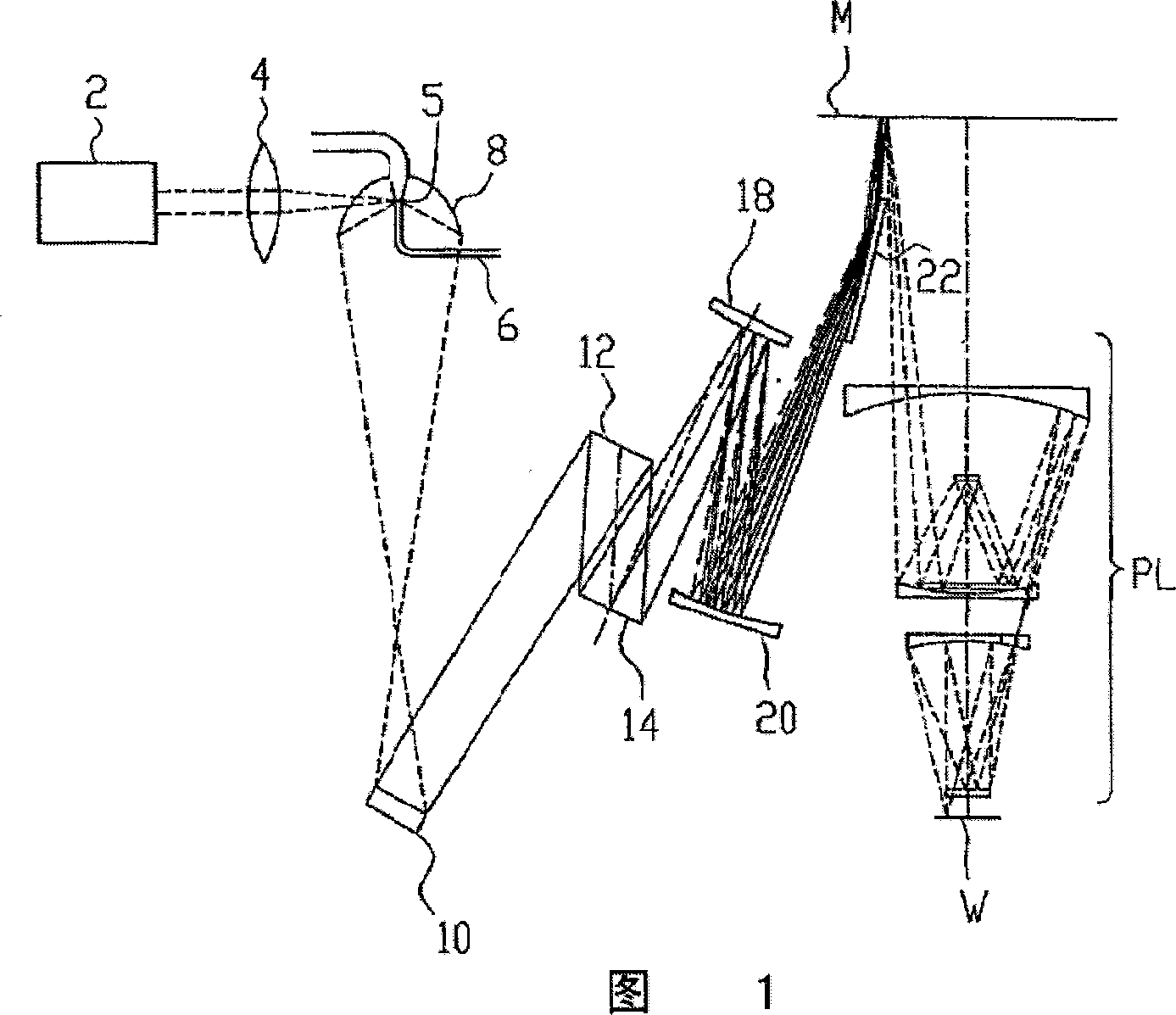
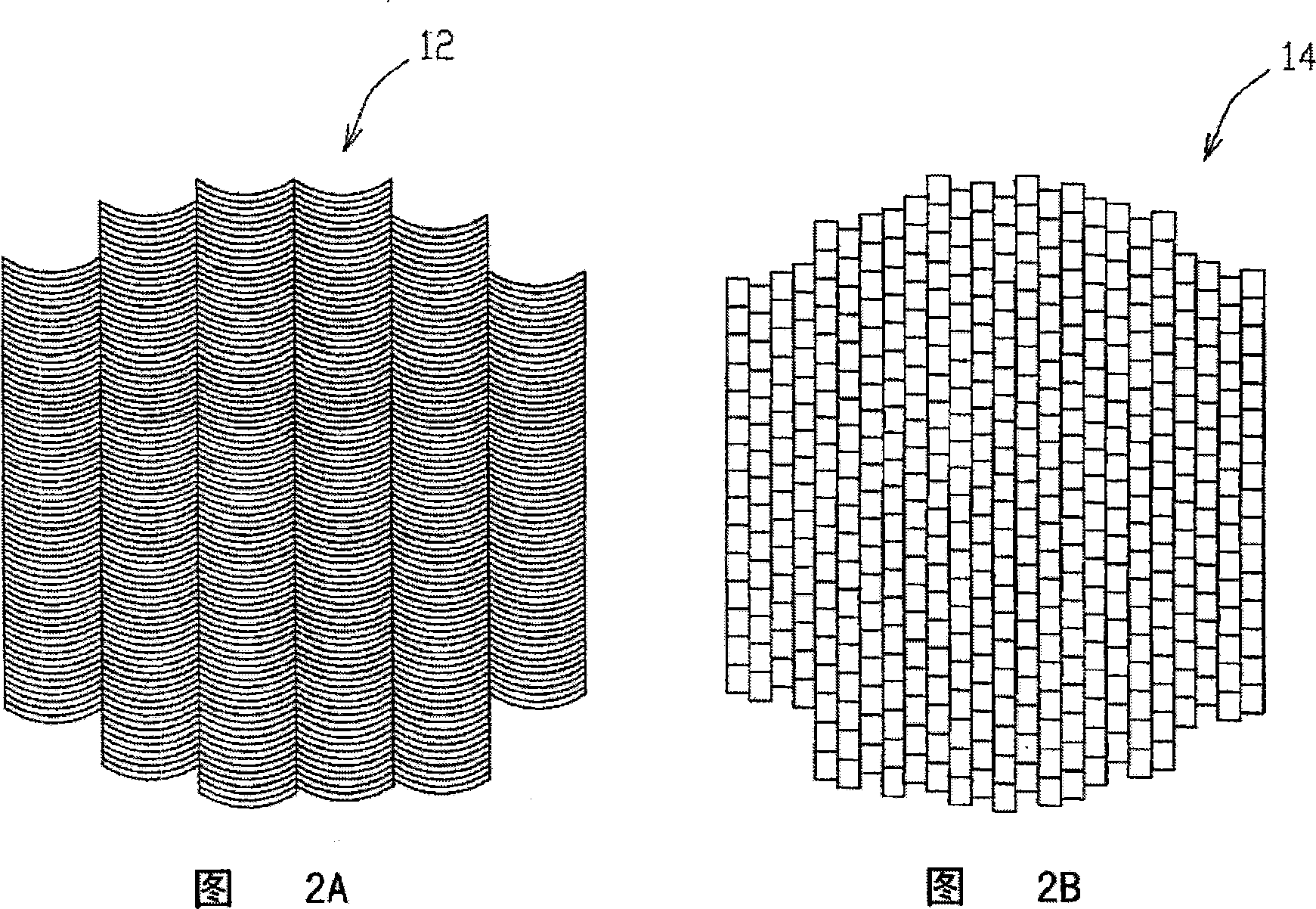
[0067] FIG. 8 shows a schematic configuration of the exit-side fly mirror surface and the condenser optical system constituting the illumination device of this embodiment, and a position diagram of the irradiated surface IMG. Furthermore, the mirror structure of the exit side fly mirror surface and the condenser optical system in this embodiment is the same as the mirror structure of the exit side fly mirror surface 14 and the condenser mirror surfaces 18, 20 of the above-mentioned embodiment shown in FIG. Similarly, when describing the exit-side fly mirror surface and the condenser optical system of the embodiment, the symbols used in the description of the exit-side fly mirror surface 14 and the condenser mirror surfaces 18 and 20 of the above-mentioned embodiment are used.

[0068]According to the format of the optical design software Code V (ORA Corporation), the data of the output-side fly mirror surface 14 and the condenser mirror surfaces 18 and 20 constituting the illum...


PUM

PropertyMeasurementUnit
refractive indexaaaaaaaaaa

Abstract

A lighting apparatus illuminates a plane (M) to be illuminated, with illuminating light projected from a light source (5). The lighting apparatus is provided with an entrance side reflection type fly's eye optical system (12) configured by arranging a plurality of reflection type partial optical systems in parallel; an outgoing side reflection type fly's eye optical system (14) configured by arranging a plurality of reflection type partial optical systems corresponding to each of the plurality of reflection type partial optical systems configuring the entrance side reflection type fly's eye optical system (12); and capacitor optical systems (18, 20) including two reflecting mirrors for guiding the illuminating light reflected by the outgoing side reflection type fly's eye optical system (14) to the plane (M). At least one of curvature centers of the two reflecting mirrors is optically decentered from a normal line at the center of a lighting area on the plane (M).

Description

technical field [0001] The present invention relates to an illumination device for manufacturing micro-elements such as semiconductor elements, liquid crystal display elements, and thin-film magnetic heads through photolithographic etching process, an exposure device equipped with the illumination device, and a micro-element using the exposure device manufacturing method. Background technique [0002] In recent years, the practical technology of projection exposure equipment, which uses extreme ultraviolet (EUV, extreme ultraviolet) light in the wavelength range of about 5 to 40 nm as exposure light and projects a mask pattern onto a photosensitive substrate, has been progressing. . In the EUVL (extreme ultraviolet light lithography) exposure device, because the glass material with higher transmittance to short-wavelength light is limited, so a reflective optical system is used (refer to, for example, U.S. Patent No. 6,452,661 specification and Japanese Patent Early public...

Claims


Application Information

Patent Timeline
Patent Type & Authority Applications(China)
IPC IPC(8): H01L21/027G02B19/00G02B5/10G03F7/20
CPCG03F7/70075G03F7/702G02B27/0905G02B27/0983G03F7/70091
Inventor 小松田秀基
Owner NIKON CORP
Why Eureka
Try Eureka