

Wave-shaped applying structure
A wave-shaped, coating technology, applied in the direction of coating non-metallic protective layers, printed circuits, instruments, etc., can solve the problems of TAB/COF lead short circuit, etc., to achieve the effect of avoiding lead short circuit, increasing the flow space and reducing accumulation
- Summary
- Abstract
- Description
- Claims
- Application Information
AI Technical Summary
Problems solved by technology
Method used
Image

Examples
Embodiment Construction
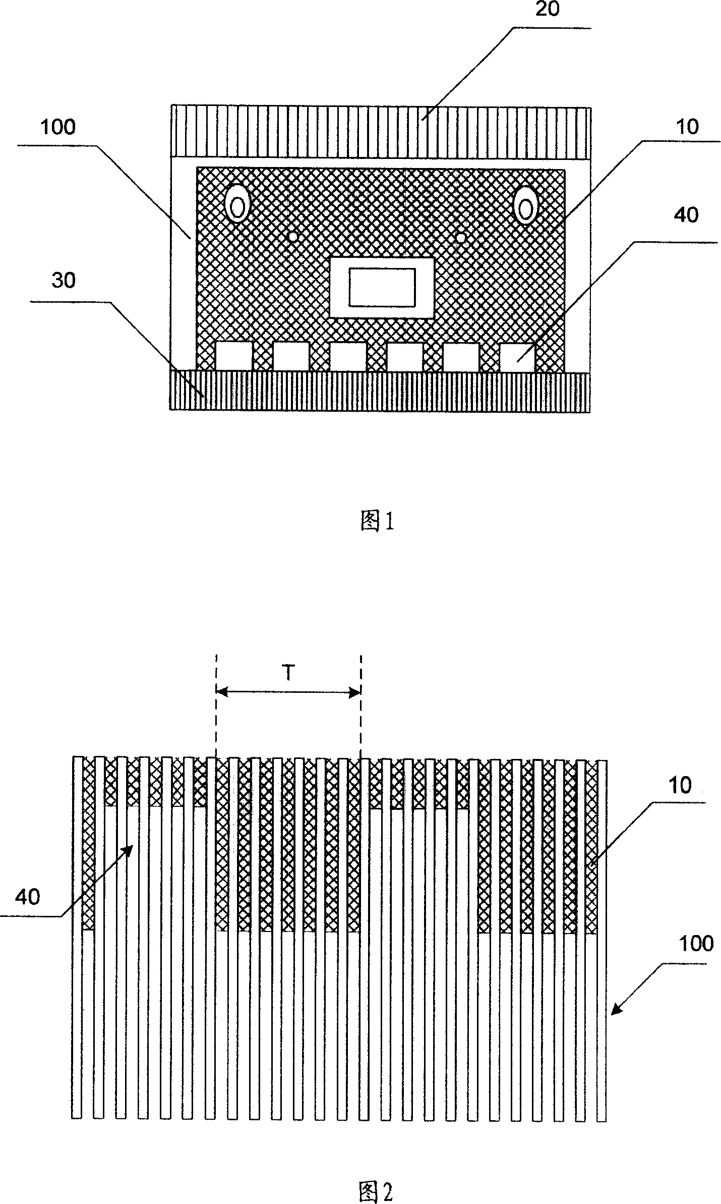
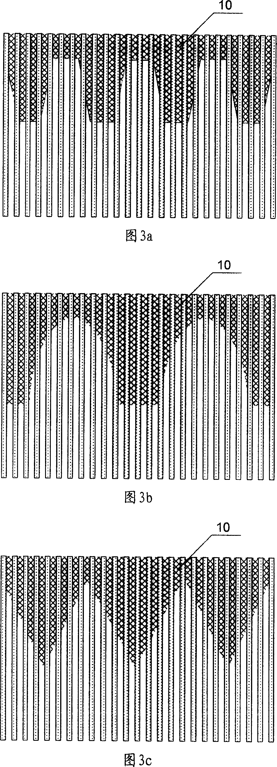
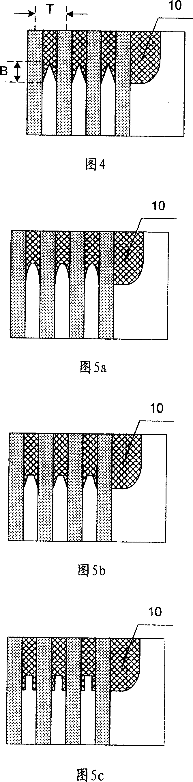
[0021] Fig. 1 is a schematic diagram of the wavy coating structure of the present invention. As shown in FIG. 1 , the S / R coating layer 10 is coated on the TAB / COF 100 , and the overall shape is still rectangular. The upper part of the TAB / COF is a printed circuit board and TAB / COF bonding (Bonding PCB) area 20 , and the lower part is a glass substrate and TAB / COF bonding (Bonding Cell) area 30 . The distance between the printed circuit board and the leads in the TAB / COF crimping area 20 is relatively large, about 400 μm, and there will be no accumulation of ACF particles. The distance between the glass substrate and the lead wires in the TAB / COF crimping area 30 is relatively small, about 60 μm, and ACF particles are likely to accumulate and cause short circuit of the TAB / COF lead wires. In the present invention, several recesses 40 are arranged on the edge of the S / R coating layer 10 in the area where the glass substrate and the TAB / COF are crimped, so that the edge of the ...
PUM
 Abstract
Description
Claims
Application Information