A making method of the contact hole plug and layer 1 metal

A manufacturing method and contact hole technology, which are used in semiconductor/solid-state device manufacturing, electrical components, circuits, etc., can solve problems such as increased plug resistance, defective semiconductor devices, and easy formation of voids, so as to improve production efficiency and reduce interconnection. Resistance, the effect of reducing manufacturing steps

Inactive Publication Date: 2007-08-15
SHANGHAI INTEGRATED CIRCUIT RES & DEV CENT
View PDF0 Cites 3 Cited by
  • Summary
  • Abstract
  • Description
  • Claims
  • Application Information

AI Technical Summary

Problems solved by technology

[0003] However, the above-mentioned contact hole plug and the first layer of metal are respectively made of tungsten and aluminum with high resistivity, so that the interconnection resistance of semiconductor devices cannot meet the continuous reduction of semiconductor device feature size requirements; in addition, through physical When vapor deposition deposits tungsten to form tungsten plugs, it is easy to form voids, which increases the resistance of the plugs and leads to poor semiconductor devices; moreover, the contact hole plugs are made separately from the first layer of metal, resulting in the entire process Many, reducing the production efficiency of semiconductor devices

Method used


Image

  • A making method of the contact hole plug and layer 1 metal
  • A making method of the contact hole plug and layer 1 metal
  • A making method of the contact hole plug and layer 1 metal

Examples


Embodiment Construction

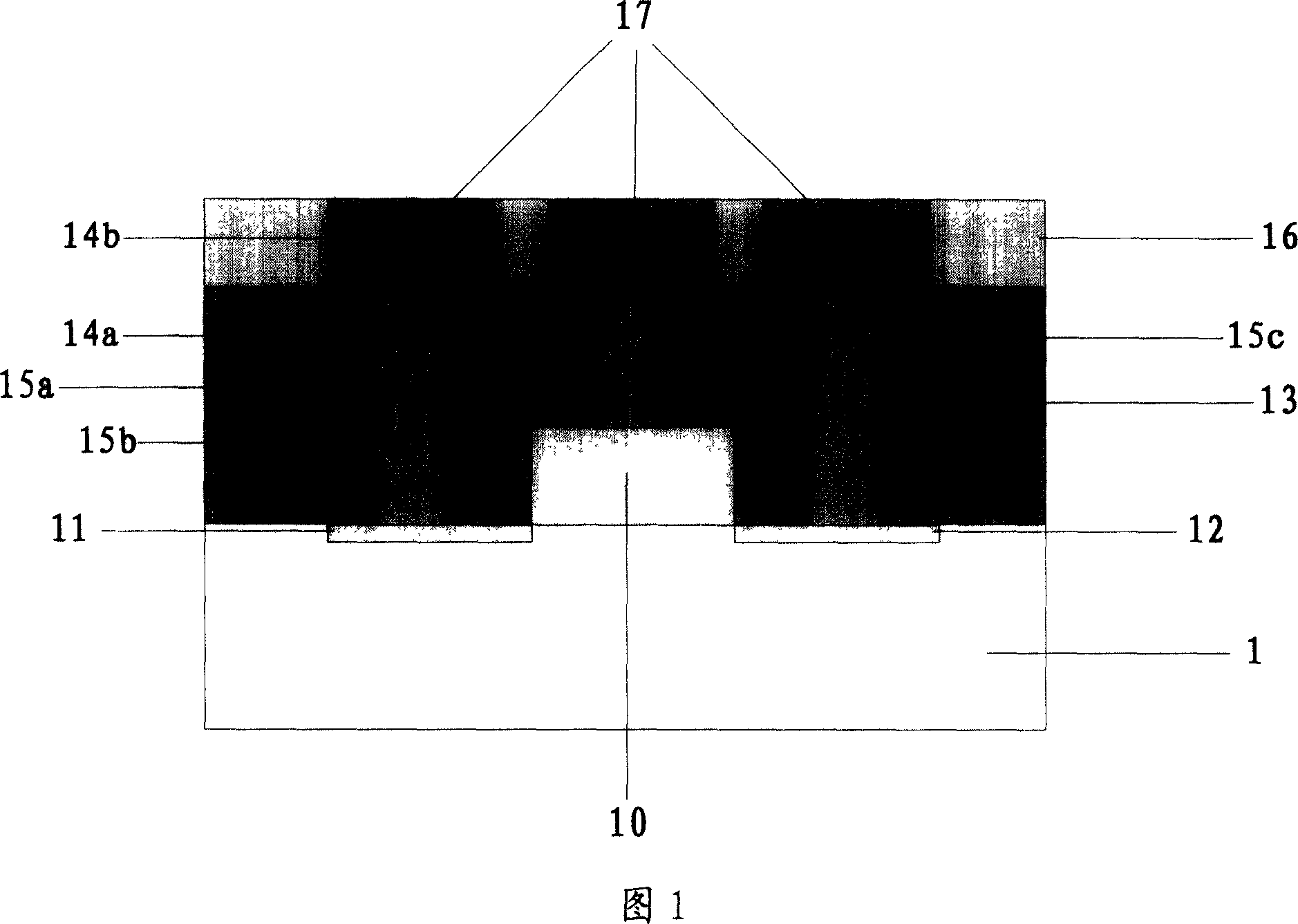
[0023] The method for manufacturing the contact hole plug and the first layer metal of the present invention will be further described in detail below.

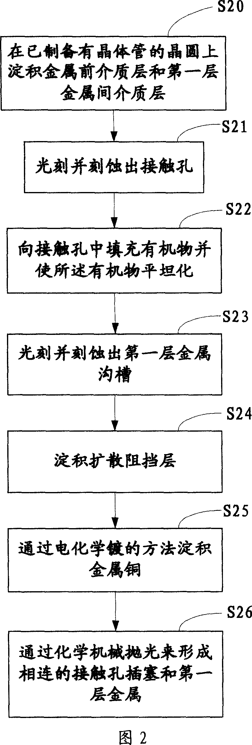
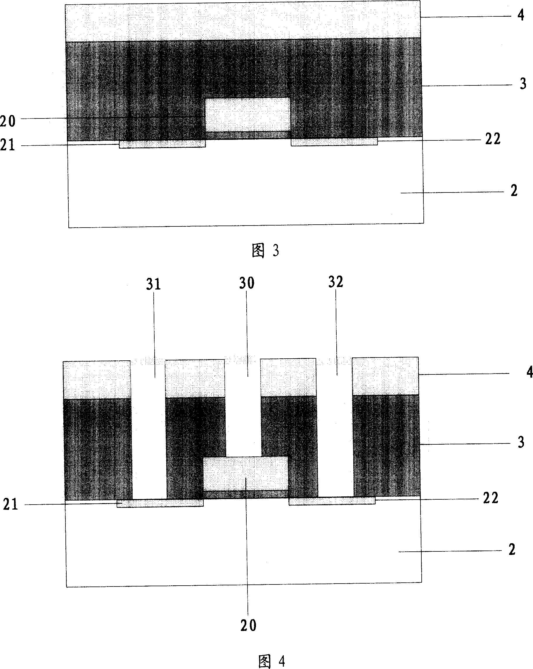
[0024] Referring to FIG. 2, the method for manufacturing the contact hole plug and the first layer of metal of the present invention first performs step S20, depositing a pre-metal dielectric layer and a first layer of intermetallic dielectric layer on the wafer prepared with transistors, wherein, The pre-metal dielectric layer and the first intermetal dielectric layer are made of different materials. In this embodiment, the metal pre-dielectric layer is firstly deposited on the wafer prepared with transistors by chemical vapor deposition, then chemical mechanical polishing is performed on the metal pre-dielectric layer, and finally the metal pre-dielectric layer is deposited on the wafer by chemical vapor deposition. A first intermetal dielectric layer is deposited on the pre-metal dielectric layer. Referring to FIG. 3 , it...


PUM


Abstract

The related preparation method for contact hole plug and first layer metal comprises: on the wafer with transistor, depositing metal front-media layer and the first metal intermediate layer; photo etching the contact hole, filling the hole with organic, and flattening the organic; photo etching the first metal groove, depositing the diffusion-barrier layer, electrochemical depositing copper, and chemical-mechanical polishing to form the plug and first layer metal. This invention overcomes defects in prior art, reduces product size, and simplifies procedure for higher efficiency.

Description

technical field [0001] The invention relates to the field of semiconductor manufacturing, in particular to a method for manufacturing a contact hole plug and a first layer of metal. Background technique [0002] The materials of the existing contact hole plug and the first metal layer are respectively tungsten and aluminum (or copper), which are manufactured separately. With reference to FIG. 1, the method for manufacturing the contact hole plugs 15a, 15b and 15c and the first layer of metal 17 specifically includes the following steps: depositing A pre-metal dielectric layer 13 is chemically mechanically polished; photolithography and etching a contact hole (not shown); a diffusion barrier layer 14a is deposited on the contact hole; metal tungsten is deposited by chemical vapor deposition (CVD) on Form tungsten plugs 15a, 15b and 15c in the contact holes; make the tungsten plugs 15a, 15b and 15c equal to the pre-metal dielectric layer 13 by chemical mechanical polishing; d...

Claims


Application Information

Patent Timeline
Patent Type & Authority Applications(China)
IPC IPC(8): H01L21/768
Inventor 康晓旭
Owner SHANGHAI INTEGRATED CIRCUIT RES & DEV CENT
Why Eureka
Try Eureka