Metal diffusion barrier layer structure and forming method thereof

A metal diffusion and metal layer technology, applied in electrical components, semiconductor/solid-state device manufacturing, circuits, etc., can solve the problems of shrinking, increasing copper interconnection resistance, increasing proportion, etc., to reduce thickness, reduce self-resistance, and good matching. Effect

Pending Publication Date: 2020-12-25
SHANGHAI INTEGRATED CIRCUIT RES & DEV CENT
View PDF0 Cites 0 Cited by
  • Summary
  • Abstract
  • Description
  • Claims
  • Application Information

AI Technical Summary

Problems solved by technology

[0005] However, with the development of CMOS technology to 5nm or even lower technology generations, the size of wires continues to shrink, so that the thickness of the barrier layer accounts for a sharp increase in the proportion of the entire cross-section of the wire, and the resistance of the barrier layer is much greater than that of copper metal. Therefore, it will cause Dramatic increase in copper interconnect resistance

Method used


Image

  • Metal diffusion barrier layer structure and forming method thereof
  • Metal diffusion barrier layer structure and forming method thereof
  • Metal diffusion barrier layer structure and forming method thereof

Examples


Embodiment Construction

[0026] The specific embodiment of the present invention will be further described in detail below in conjunction with the accompanying drawings.

[0027] It should be noted that, in the following specific embodiments, when describing the embodiments of the present invention in detail, in order to clearly show the structure of the present invention for the convenience of description, the structures in the drawings are not drawn according to the general scale, and are drawn Partial magnification, deformation and simplification are included, therefore, it should be avoided to be interpreted as a limitation of the present invention.

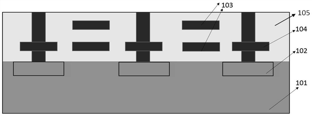
[0028] In the following specific embodiments of the present invention, please refer to Figure 7 , Figure 7 It is a metal diffusion barrier layer structure manufactured according to a metal diffusion barrier layer structure forming method of the present invention in a preferred embodiment of the present invention. Such as Figure 7 As shown, a ki...


PUM

PropertyMeasurementUnit
thicknessaaaaaaaaaa
thicknessaaaaaaaaaa
thicknessaaaaaaaaaa

Abstract

The invention discloses a metal diffusion barrier layer structure. The metal diffusion barrier layer structure sequentially comprises a first metal layer, a first graphene layer, a second metal layerand a second graphene layer which cover the inner wall surface of a groove or a hole, wherein the first graphene layer and the second graphene layer are respectively formed on the interfaces of the first metal layer and the second metal layer and the interfaces of the second metal layer and the third metal layer by injecting carbon into the second metal layer for doping and carrying out heat treatment so as to replace traditional tantalum nitride to be used as metal diffusion prevention layers, so that the thickness of the barrier layer can be greatly reduced; the proportion of the metal wirelayer on the conductive section is increased, the metal interconnection resistance can be greatly reduced on the whole, the electromigration resistance of the wire is improved, the process integrationis simple, and the method is compatible with the CMOS process. The invention further discloses a forming method of the metal diffusion barrier layer structure.

Description

technical field [0001] The invention relates to the technical field of semiconductor integrated circuit technology, in particular to a metal diffusion barrier layer structure and a forming method that can be used in subsequent interconnection technologies. Background technique [0002] In VLSI technology, with the miniaturization of devices and the improvement of integration, the number of conductor connections in the circuit is also increasing, making the resistance (R) and capacitance (C) in the conductor connection structure generated The parasitic effect also expands accordingly, and caused serious transmission delay (RC delay) problem. [0003] In terms of reducing wire resistance, metal copper has been widely used in wiring structures to replace metal aluminum as a conductor wiring material because of its high melting point, low resistivity and high resistance to electromigration. [0004] However, since copper is easy to diffuse in the dielectric layer, resulting in ...

Claims


Application Information

Patent Timeline
Patent Type & Authority Applications(China)
IPC IPC(8): H01L21/768
CPCH01L21/76828H01L21/76832H01L21/76877
Inventor 朱建军林威豪武青青
Owner SHANGHAI INTEGRATED CIRCUIT RES & DEV CENT
Why Eureka
Try Eureka