Semiconductor device and manufacturing method thereof

一种制造方法、半导体的技术,应用在半导体/固态器件制造、半导体器件、晶体管等方向,能够解决NPN晶体管难以得到高频特性及电流增幅率、扩散深度深、基极电阻值变高等问题,达到提高高频特性及电流增幅率、减小基极电阻值、减小集电极电阻值的效果

Inactive Publication Date: 2007-08-29
SANYO ELECTRIC CO LTD
View PDF2 Cites 2 Cited by
  • Summary
  • Abstract
  • Description
  • Claims
  • Application Information

AI Technical Summary

Problems solved by technology

However, the diffusion layer used as the internal base region has a low concentration and a deep diffusion depth, resulting in a high base resistance value, which makes it difficult to obtain the desired high-frequency characteristics and current amplification rate of the NPN transistor.

Method used


Image

  • Semiconductor device and manufacturing method thereof
  • Semiconductor device and manufacturing method thereof
  • Semiconductor device and manufacturing method thereof

Examples


Embodiment Construction

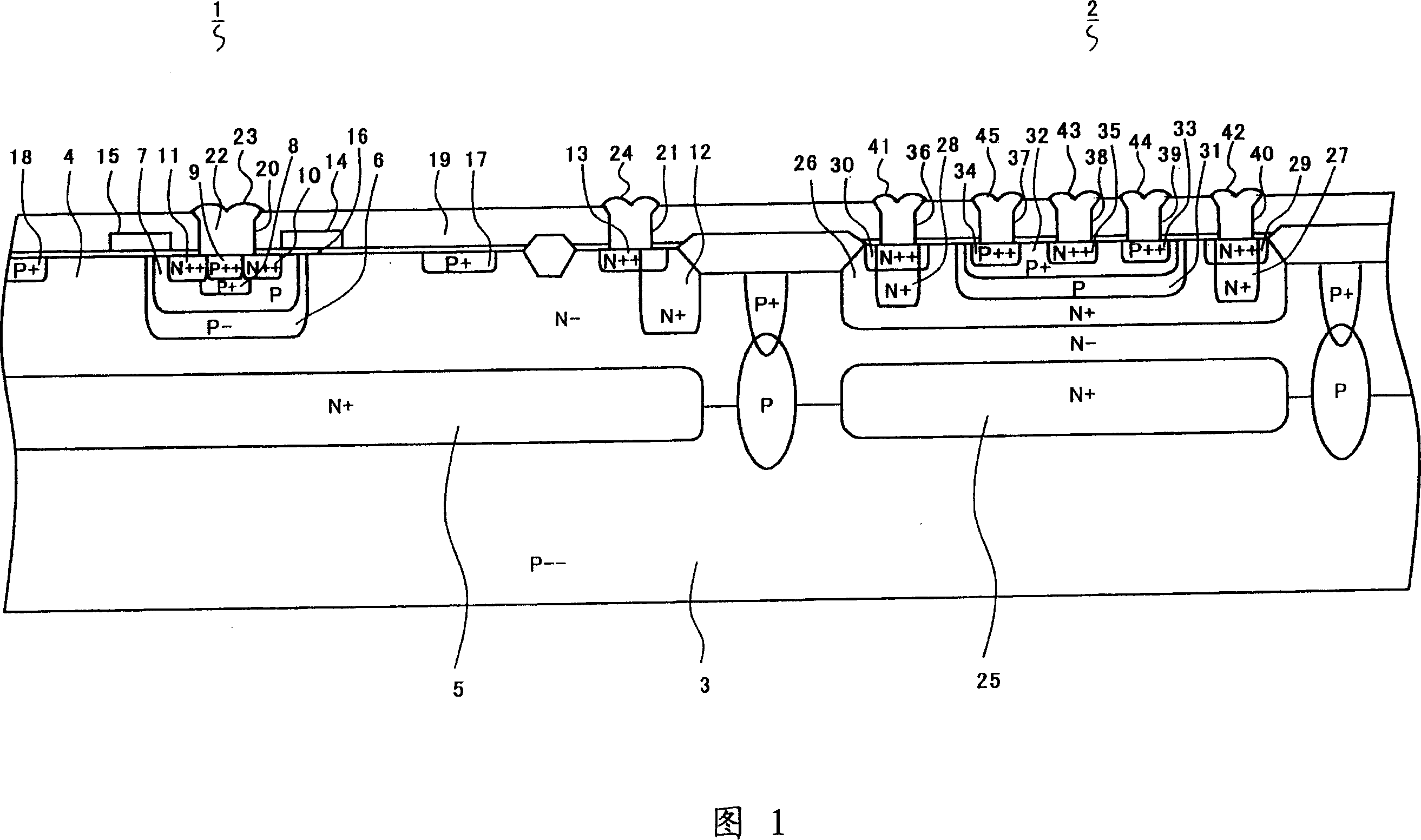
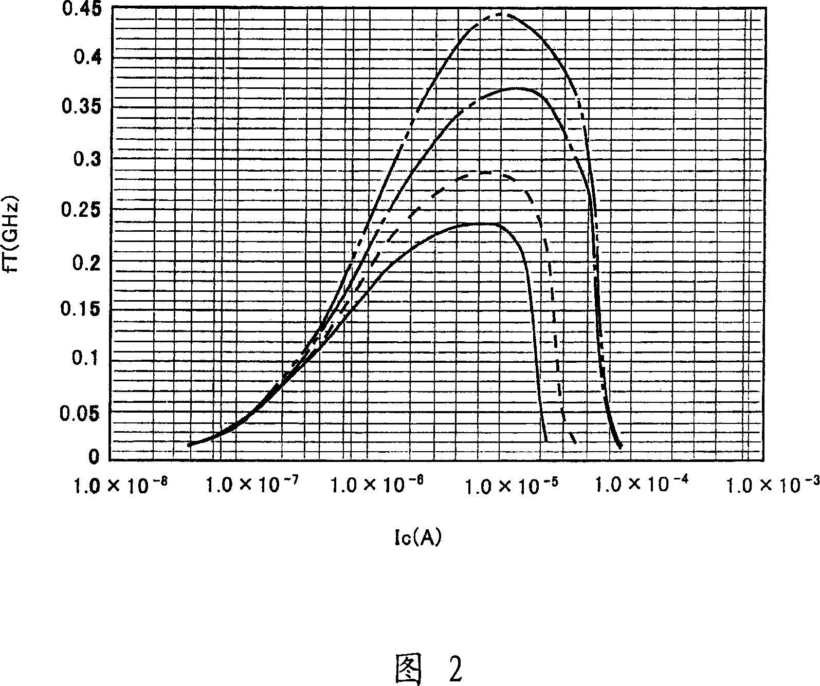
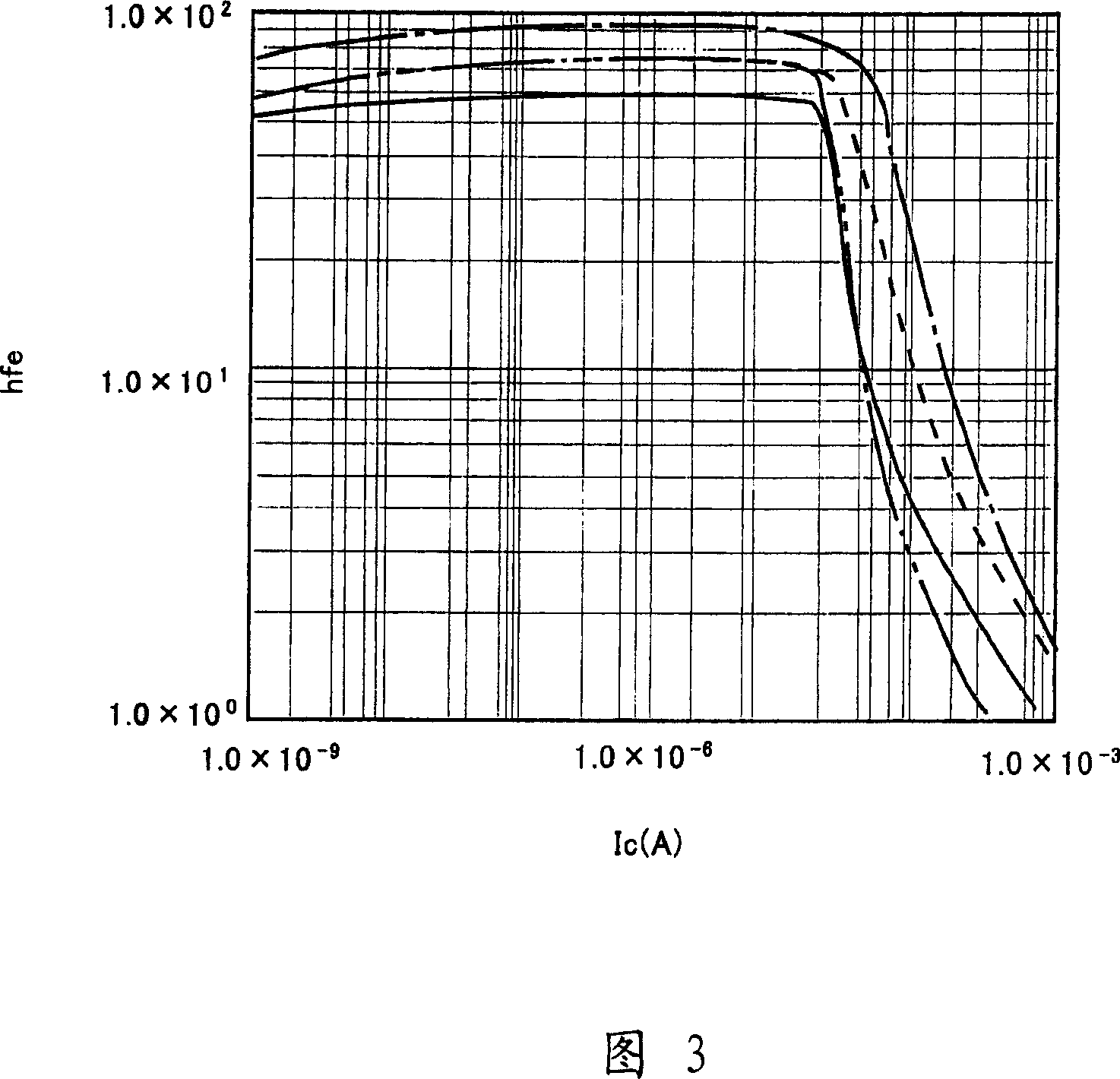
[0042] Hereinafter, a semiconductor device according to an embodiment of the present invention will be described in detail with reference to FIGS. 1 to 4 . FIG. 1 is a cross-sectional view illustrating a semiconductor device according to the present embodiment. FIG. 2 is a diagram illustrating the relationship between the cutoff frequency (fT) and the collector current (Ic) of the semiconductor device according to the present embodiment. FIG. 3 is a graph illustrating the relationship between the current amplification factor (hfe) and the collector current (Ic) of the semiconductor device according to the present embodiment. 4 is a diagram illustrating the relationship between collector-emitter current (Ice) and collector-emitter voltage (Vce) of the semiconductor device according to the present embodiment.

[0043] As shown in FIG. 1 , an N-channel MOS transistor 1 and an NPN transistor 2 are formed on the same P-type single crystal silicon substrate 3 . In addition, in the...


PUM


Abstract

The present invention provides a semiconductor device. In the existing semiconductor device, high break down voltage NPN transistor with high frequency characteristics is difficult formed. In the semiconductor device of the present invention, an N type epitaxial layer (4) is formed on a P type silicon substrate (3). In the N type epitaxial layer (4), P type diffusion layers (31, 32) as a base region, N type diffusion layers (27-30) as collector regions and an N type diffusion layer (35) as an emitter region are formed. In this event, the P type diffusion layers (31-32) are formed so as to have a double diffusion structure, and an impurity concentration in a surface of the base region and in a region adjacent thereto is set high. This structure enables improvement in high frequency characteristics and in a current amplification factor while maintaining breakdown voltage characteristics of an NPN transistor (2).

Description

technical field [0001] The invention relates to a semiconductor device aimed at improving the high-frequency characteristics and current amplification rate of a transistor. Background technique [0002] As an example of a conventional semiconductor device and its manufacturing method, the following NPN transistor is known. On the P-type silicon semiconductor substrate, an N-type epitaxial layer is formed. On the epitaxial layer, an extrinsic base region is formed around it in such a way as to surround the active base region. The extrinsic base region is connected to the extrinsic base extraction electrode formed on the epitaxial layer. Furthermore, an emitter region is formed on the active base region, and the emitter region is connected to an emitter extraction electrode. In addition, a collector region is formed on the epitaxial layer. At this time, impurities in the extrinsic base extraction electrode are diffused into the epitaxial layer to form an extrinsic base reg...

Claims


Application Information

Patent Timeline
Patent Type & Authority Applications(China)
IPC IPC(8): H01L29/73H01L21/822
CPCH01L29/7322H01L29/1004H01L27/0623H01L21/8249H01L29/0804
Inventor 中谷清史
Owner SANYO ELECTRIC CO LTD
Why Eureka
Try Eureka