Production of high-brightness light-emitting diodes chip

A light-emitting diode, high-brightness technology, applied in electrical components, circuits, semiconductor devices, etc., can solve the problems of reducing yield, damage, cracking, etc., to improve the pass rate, avoid damage, and increase production efficiency.

Inactive Publication Date: 2007-09-05
Shandong Huaguang Optoelectronics Co. Ltd.
View PDF0 Cites 22 Cited by
  • Summary
  • Abstract
  • Description
  • Claims
  • Application Information

AI Technical Summary

Problems solved by technology

During the half-cutting process, due to the high-speed rotation of the diamond knife grinding wheel and the hard contact with the GaAs material, a large number of cracks are generated during the half-cutting process, which is a relatively large damage to the luminous PN junction, and will seriously cause Reverse leakage, lower yield

Method used


Image

  • Production of high-brightness light-emitting diodes chip
  • Production of high-brightness light-emitting diodes chip
  • Production of high-brightness light-emitting diodes chip

Examples


Embodiment

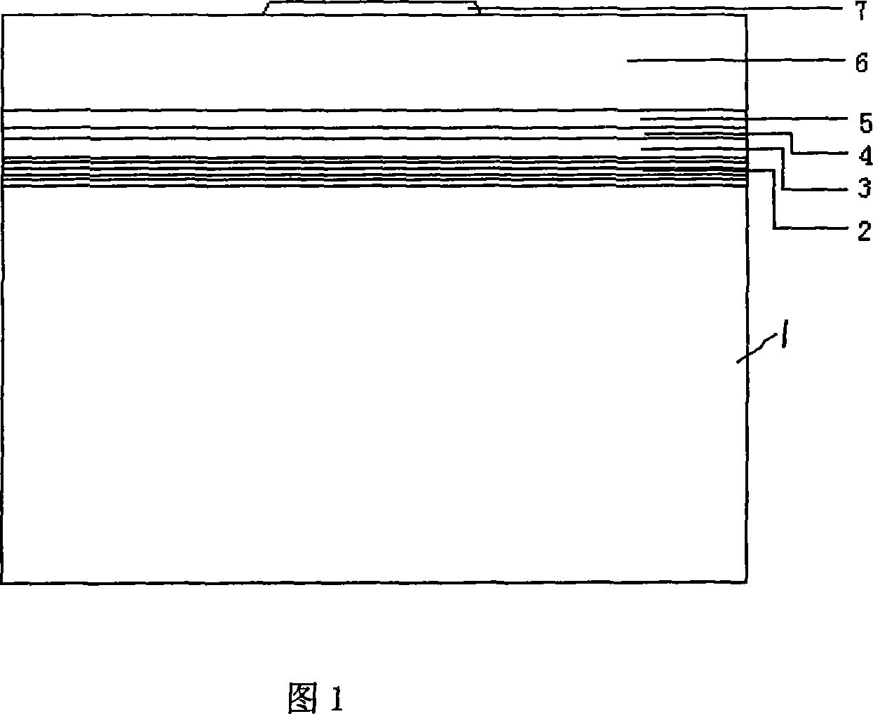
[0024] The invention uses the photoresist as the corrosion protection layer, and through the methods of selective exposure, development and chemical corrosion, completes the negative pole of the GaAs substrate and separates the positive pole of the light-emitting diode chip. Specifically, after the conventional LED process is done, the following steps are carried out before testing:

[0025] 1. Uniform glue: evenly coat positive photoresist on the surface of the LED epitaxial wafer. Carry out on the homogenizer, the speed of the homogenizer is 4000 rpm, and the time is 20 seconds.

[0026] 2. Baking: put the light-emitting diode epitaxial wafer coated with positive photoresist into an oven, and bake at a temperature of 100-150 degrees for 10-30 minutes.

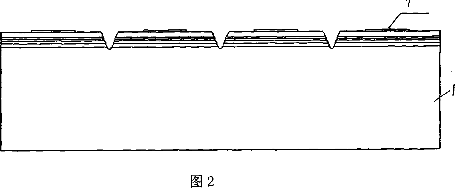
[0027] 3. Exposure: exposure on a UV lithography machine, the mask pattern is shown in Figure 5, align with the original electrode pattern, and expose in the exposure area 8 with a width of 20 to 50 microns between each chip...


PUM


Abstract

The invention is concerned with production to a kind of high brightness light-emitting diode chip. It adopts etching method to replace half-cutting process and etching glue as corrosion protection layer to prepare GaAs underlay cathode and separate anode of light-emitting diode chip, through selecting exposal, develop and chemical etching technique. Before taking the test and after carrying routine process, treat the light-emitting diode chip with such steps, (1) spare (2) firing, (3) exposal, (4) develop, (5) firing, (6) corrosion. This method takes chemical etching technique to replace the half-cutting process, only carried the cutting of separation of chip without touching PN junction to avoid the rigid damage of PN junction, thus it increases the qualified rate of device and produces efficiency to one time. The light-emitting area of PN junction made by chemical etching is a whole bowl-shape table board and is fit for emitting light to all directions, and the light-emitting brightness of LED chip increases 10 percent.

Description

technical field [0001] The invention relates to a method for preparing a light-emitting diode. Background technique [0002] As a new type of high-efficiency solid-state light source, high-brightness light-emitting diodes (LEDs) have significant advantages such as high luminous efficiency, small size, light weight, long life, energy saving, safety, green environmental protection, and fast response. Signal lights, large-screen displays, automotive signal lights and lighting are playing an increasingly important role. High-brightness light-emitting diodes can be divided into red, yellow, blue, green, etc. according to their colors. Using MOCVD epitaxy to grow InGaN, GaN and other structures on silicon carbide and sapphire substrates can obtain blue and green high-brightness light-emitting diodes; epitaxial AlGaInP materials on GaAs substrates can obtain color coverage from red, orange, yellow, to yellow LEDs in the green band. [0003] Since high-brightness LED dies are mai...

Claims


Application Information

Patent Timeline
Patent Type & Authority Applications(China)
IPC IPC(8): H01L33/00
Inventor 任忠祥夏伟徐现刚李树强
Owner Shandong Huaguang Optoelectronics Co. Ltd.
Why Eureka
Try Eureka