Material for covering outside of deivce and manufacturing method thereof

A technology of covering device and manufacturing method, which is applied in the directions of lamination device, chemical instrument and method, electrical equipment shell/cabinet/drawer, etc., can solve the problem that the notebook computer shell cannot adopt the die-casting process, consumes manpower and cost, and leaks electromagnetic waves. And other issues

Inactive Publication Date: 2007-10-03
SAN FANG CHEM IND
View PDF0 Cites 8 Cited by
  • Summary
  • Abstract
  • Description
  • Claims
  • Application Information

AI Technical Summary

Problems solved by technology

[0022] Although titanium alloy material has the above-mentioned advantages when applied to notebook computers, the die-casting process cannot be used to manufacture notebook computer casings from titanium alloys, but the stamping process can only be used. Since the crystal structure of titanium metal is HCP, the mechanical properties of the material are relatively brittle. Therefore, the stamping process also has its difficulties; when the titanium alloy notebook computer case is manufactured by the stamping process, it can only be manufactured in pieces. There are many strong ribs in the notebook computer case, and the case is connected with other parts. The connecting part of the shell, the connecting part of the shell and the shell, etc., these parts need to be manufactured separately and then connected by bonding and sheet metal. The number of secondary processing processes is too many, which requires a lot of manpower and cost.
[0023] Based on the above reasons, the shell materials of electronic products on the market mainly include ABS plastic, aluminum-magnesium alloy, carbon fiber and titanium alloy. Generally speaking, although the more popular materials in the market are aluminum-magnesium alloy and titanium alloy, but The biggest advantage of ABS plastic material is the plastic injection process, which has low cost and fast manufacturing. There are many reinforcing ribs in the housing of electronic products, the connection between the housing and other parts, the connection between the housing and the housing, etc. , can be completed at one time by the plastic injection process, but it cannot meet the strength requirements of the shells in today's electronic products, and cannot solve the problem of electromagnetic wave leakage in electronic products; there are also many problems encountered by aluminum-magnesium alloys. In terms of productivity, the defect rate of magnesium-aluminum alloy die-casting is extremely high, and the number of secondary processing process

Method used


Image

  • Material for covering outside of deivce and manufacturing method thereof
  • Material for covering outside of deivce and manufacturing method thereof
  • Material for covering outside of deivce and manufacturing method thereof

Examples


Embodiment 1

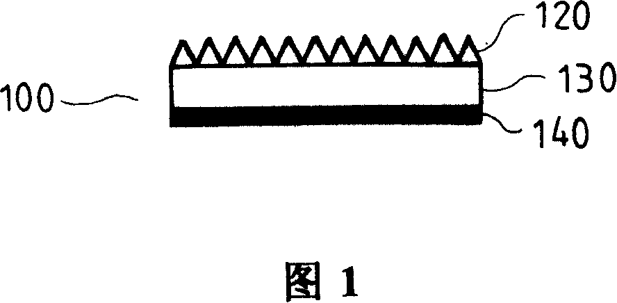
[0054] After preparing the textured release paper, coat the colored PU fabric layer on the release paper. After the fabric layer is coated, dry it, and then apply the PU coating layer, and wait for it to dry to form a structure After the layer 130, apply the last PU paint primer as the primer layer 140. After the steps of drying, winding and aging, the release paper is released to form the surface layer 120, and a PU with surface color lines can be obtained. The surface electronic covering material, as shown in Figure 1, has a specification of total thickness of 0.5mm; PU coating layer porosity of 0%; softness and hardness ShoreA: 60.

Embodiment 3

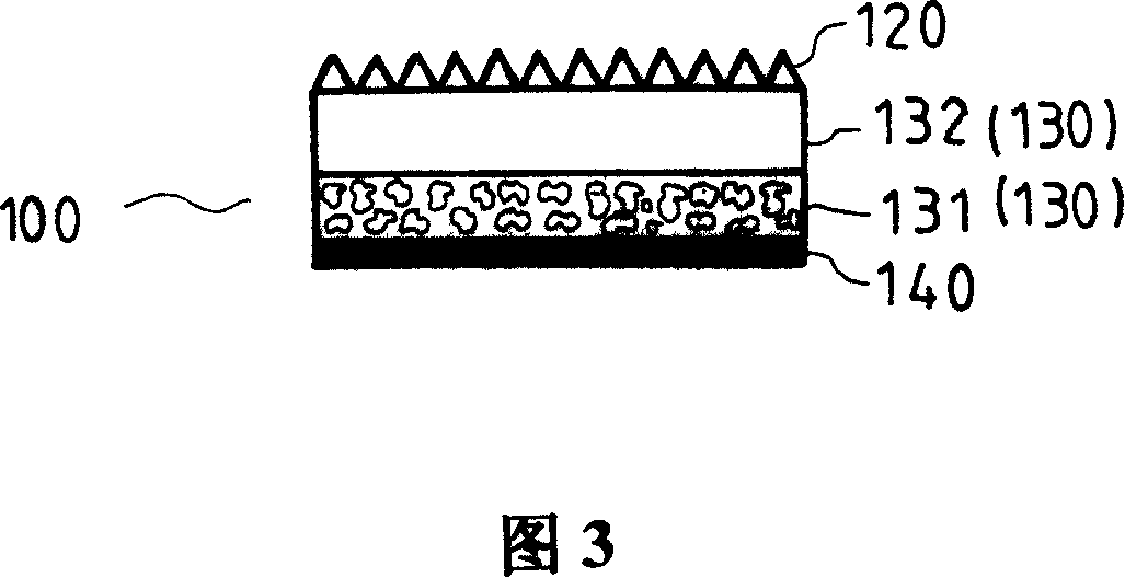
[0058] In the third embodiment of the present invention, after the release paper with texture is prepared, the PU fabric layer with color is coated on the release paper. After the fabric layer is coated, it is dried, and then the PU is coated. Paint layer, after it is dried to form a PU non-foaming structure layer 132, coat the PU paint layer adding foaming agent, after it is dried to form a PU foaming structure layer 131, coat the last PU coating The bottom layer is used as the bottom layer 140. After the steps of drying, winding and aging, the release paper is released to form the surface layer 120, and an electronic covering material with a PU appearance with surface color lines can be obtained, and the structural layer 130 It has a structure of PU foamed structural layer 131 and PU non-foamed structural layer 132, and the structural layer next to the surface layer 120 is PU non-foamed structural layer 132, as shown in Figure 3, its specification is a total thickness of 0.6m...

no. 5 example

[0062] In the fifth embodiment of the present invention, first prepare the release cloth, apply the PU wet paint, put it into water to solidify the PU wet paint, rinse with water after solidification, curl after drying, and grind the surface After tearing off the release cloth, a fuzzy PU surface electronic covering material can be formed; its specification is a total thickness of 0.4mm; the porosity of the PU layer is 30%; the hardness ShoreA: 15.

[0063] To sum up, the material for covering the surface of the device and its manufacturing method of the present invention not only achieve the expected practical effect, but also have an unprecedented design, which meets the requirements of the patent law invention, so the application is filed in accordance with the law. For this reason, I would like to ask your reviewers to review in detail, and pray for the patent application as soon as possible, so thank you for your convenience.


PUM

PropertyMeasurementUnit
Thicknessaaaaaaaaaa
Total thicknessaaaaaaaaaa
Hardness degreeaaaaaaaaaa

Abstract

The invention relates to one kind of coating material and its manufacturing method. The manufacturing method is that: it covers PU fabric layer on the detachable base-paper, after its drying, and then it covers PU bottom layer. After drying, coiling and cooking, it detaches the detachable base-paper off to achieve the PU covering material with colorful texture. In the invention, the surface layer with at least one colorful texture layer and the PU basal layer can be used for covering electronic products, which can increases users' good feeling for electronic products.

Description

technical field [0001] The invention relates to a material for covering the appearance of a device and a manufacturing method thereof, especially to a material characteristic such as a variety of textures and color changes on the surface of a PU material, which is used to cover the appearance of electronic products, so that it has a soft, comfortable touch, and an appearance similar to genuine leather. Diversity and other characteristics. Background technique [0002] The housing materials of electronic products on the market mainly include ABS plastic, aluminum-magnesium alloy, carbon fiber and titanium alloy. Generally speaking, the most popular materials in the market are aluminum-magnesium alloy and titanium alloy. Both have their advantages and disadvantages. The following is a comparison of the characteristics of these materials: [0003] Type 1: Fireproof plastic-ABS [0004] ABS is made of styrene, acrylonitrile and butadiene emulsion copolymerization. Its heat res...

Claims


Application Information

Patent Timeline
IPC IPC(8): H05K5/00B32B27/00B32B37/00
Inventor 冯崇智姚伊蓬黄培火王格峰林永松康开丰
Owner SAN FANG CHEM IND
Why Eureka
Try Eureka