
Method for local bonding silicon / glass by laser

A glass laser and bonding technology, which is applied in semiconductor/solid-state device manufacturing, electrical components, circuits, etc., can solve the problems of limited application, device pollution, high annealing temperature, etc., and achieve good bonding area selectivity and overall bonding The effect of low temperature and strong process controllability

Inactive Publication Date: 2007-10-10
HUAZHONG UNIV OF SCI & TECH
View PDF0 Cites 14 Cited by
  • Summary
  • Abstract
  • Description
  • Claims
  • Application Information

AI Technical Summary

Problems solved by technology

Silicon fusion bonding is mostly used in SOI technology, such as Si-SiO 2 bonding and Si-Si bonding, however, the bonding process requires a higher annealing temperature
The temperature of anodic bonding is 200-400 degrees, which is lower than that of direct / eutectic bonding, however it needs a strong electric field of 1000-2000V to achieve high-quality bonding, and strong electric fields will threaten microcircuits, and The alkali ions of the glass in anodic bonding may contaminate the device, and the strict requirements of bonding on the flatness of the wafer surface also limit its application in MEMS manufacturing
[0004] Therefore, although direct / eutectic bonding and anodic bonding can achieve high bonding strength under high temperature and high pressure conditions, they are not suitable for the bonding of pressure, chemical and thermal sensing MEMS devices that have integrated metal thin films. co-package
At present, more and more researchers are working on using wafer surface activation treatment to reduce the external auxiliary field strength of anodic bonding and fusion bonding, but they all need to be heated on the whole device or substrate, which will lead to ineffective Necessary stress and temperature field distribution, and the above-mentioned bonding technology is not easy to achieve selective bonding, and the bonding area and heat-affected zone are difficult to control

Method used


Image

  • Method for local bonding silicon / glass by laser
  • Method for local bonding silicon / glass by laser
  • Method for local bonding silicon / glass by laser

Examples


Embodiment 1

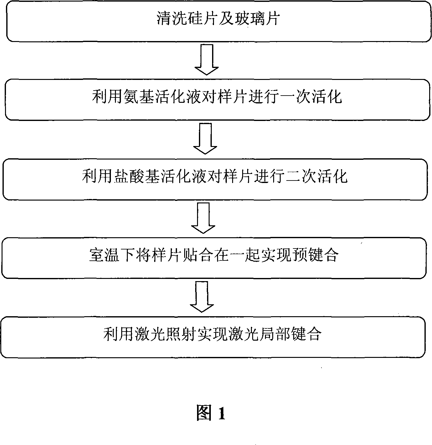
[0031] 1. Clean the sample, soak the sample to be bonded in the cleaning solution (H 2 SO 4 :H 2 o 2 =2:1), control the temperature at 120°C, and wash for 20 minutes;

[0032] 2. Soak the sample to be bonded in the amino activation solution (NH 4 OH:H 2 o 2 :H 2 (0=1:1:5) was activated once, the activation temperature was 70°C, and the sample was activated for 20 minutes;

[0033] 3. Soak the sample to be bonded in hydrochloric acid-based activation solution (HCl:H 2 o 2 :H 2 O=1:1:5) for secondary activation, the activation temperature is 70°C, and the sample is activated for 20 minutes;

[0034] 4. After drying the activated silicon wafer and glass wafer, they are quickly pasted together at room temperature to make them pre-bonded;

[0035] 5. Use the Nd:YAG laser produced by Rofin-Sinar, Germany, and adopt the continuous laser emission method for local laser bonding. The laser parameters selected for bonding are: laser power 75W, wavelength 1064nm, spot diameter...

Embodiment 2

[0038] 1. Sample cleaning. Soak the sample to be bonded in the cleaning solution (H 2 SO 4 :H2 o 2 =2:1), control the temperature at 120°C, and wash for 20 minutes;

[0039] 2. Activate the sample once. Soak the sample to be bonded in the amino activation solution (NH 4 OH:H 2 o 2 :H 2 O=1:1:5), the activation temperature is 70°C, and the sample is activated for 20 minutes;

[0040] 3. Perform secondary activation on the sample. Soak the sample to be bonded in a hydrochloric acid-based activation solution (HCl:H 2 o 2 :H 2 O=1:1:5), the activation temperature is 70°C, and the sample is activated for 20 minutes;

[0041] 4. Sample pre-bonding. After the silicon wafer and the glass wafer are blown dry, they are quickly bonded together at room temperature, and pre-bonding occurs;

[0042] 5. Local laser bonding. The laser power is 90W, the wavelength is 1064nm, the spot diameter is 200μm, and the laser scanning speed is 10mm / s.

[0043] Figure 5 is a diagram of th...

Embodiment 3

[0045] 1. Sample cleaning. Soak the sample to be bonded in the cleaning solution (H 2 SO 4 :H 2 o 2 =4:1), control the temperature at 50°C, and wash for 30 minutes;

[0046] 2. Activate the sample once. Soak the sample to be bonded in the amino activation solution (NH 4 OH:H 2 o 2 :H 2 O=1:1:3), the activation temperature is 50°C, and the sample is activated for 30 minutes;

[0047] 3. Perform secondary activation on the sample. Soak the sample to be bonded in a hydrochloric acid-based activation solution (HCl:H 2 o 2 :H 2 O=1:1:3), the activation temperature is 50°C, and the sample is activated for 30 minutes;

[0048] 4. Sample pre-bonding. After the silicon wafer and the glass wafer are blown dry, they are quickly bonded together at room temperature, and pre-bonding occurs;

[0049] 5. Local laser bonding. The laser power is 25W, the wavelength is 1064nm, the spot diameter is 200μm, and the laser scanning speed is 0.5mm / s.


PUM


Abstract

This invention discloses a method for laser local bonding of silicon / glass. The method comprises: washing, performing a first activation, performing a second activation, pre-bonding, and laser heating. After surface activation treatment, glass and silicon wafer can be intimately bonded by laser local bonding without the need for outside force. The method realizes laser local bonding through local high temperature in a certain region, and has a high bonding strength. As a whole, the silicon wafer has a low temperature, and does not have unnecessary temperature gradient or stress field distribution. Thus, the properties of the integrated pressure or temperature sensor are not influenced. The method has such advantages as simple apparatus, easy local temperature control, and high bonding efficiency.

Description

technical field [0001] The invention belongs to wafer bonding technology, in particular to a silicon / glass laser partial bonding method. Background technique [0002] Since silicon was found to have good mechanical properties and can be processed into microstructures by various processes, it has been widely used in sensor manufacturing; Integrated circuits in silicon-based microsystems for sensing or performing functions become possible; and glass has electrical insulation, good light transmission, high mechanical strength and chemical stability. Therefore, silicon and glass are used in micro-electromechanical systems MEMS (Micro Electro MechanicalSystem) has been widely used in manufacturing, and the bonding technology between silicon and glass is one of the key technologies that determine the success of MEMS packaging. [0003] At present, the bonding technologies of silicon and glass mainly include direct / eutectic bonding technology and anodic bonding technology. Direct...

Claims


Application Information

Patent Timeline
Patent Type & Authority Applications(China)
IPC IPC(8): C03C27/00H01L21/02
Inventor 史铁林廖广兰汤自荣马子文聂磊林晓辉彭平
Owner HUAZHONG UNIV OF SCI & TECH
Learn More