Large area micro nano structure soft impression method

A technology of micro-nano structure and soft embossing, which is applied in the direction of photolithography, optics, and opto-mechanical equipment on the patterned surface. Quickly and batch copy imprinting and other issues to achieve the effect of ensuring consistency

Inactive Publication Date: 2007-10-10
INST OF OPTICS & ELECTRONICS - CHINESE ACAD OF SCI
View PDF0 Cites 15 Cited by
  • Summary
  • Abstract
  • Description
  • Claims
  • Application Information

AI Technical Summary

Problems solved by technology

[0006] However, the key point of the above method is the self-assembled polymer material of SAM. When the material is printed on the metal film, the SAM will spread like ink, which will affect the resolution and line width of the transfer.
At present, the minimum line width that can be achieved abroad is about 50-100nm, which is far smaller than the structural scale that can be produced by hard imprinting technology.

Method used


Image

  • Large area micro nano structure soft impression method
  • Large area micro nano structure soft impression method
  • Large area micro nano structure soft impression method

Examples


Embodiment 1

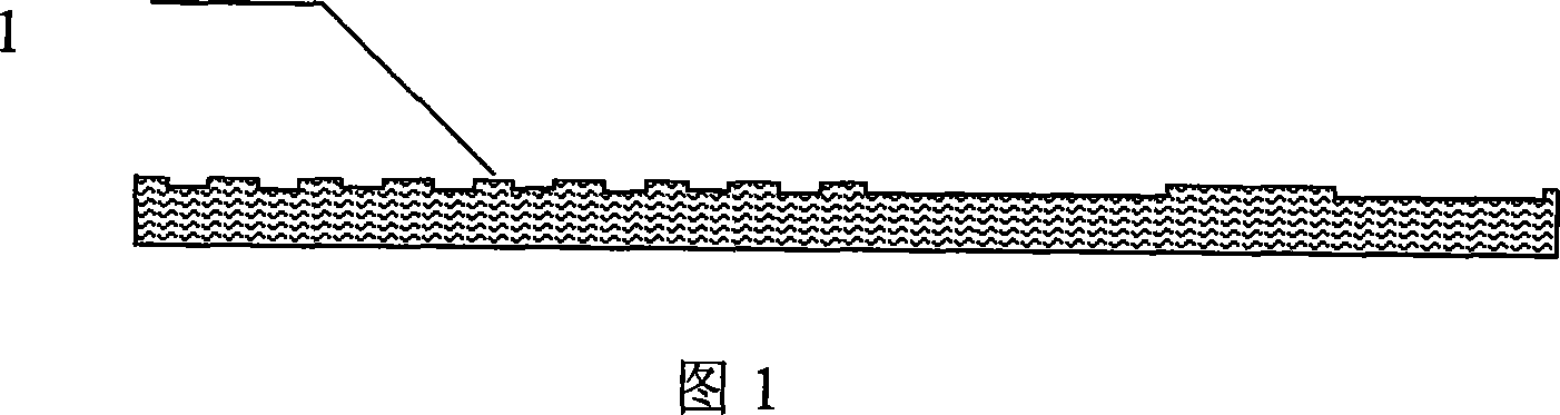
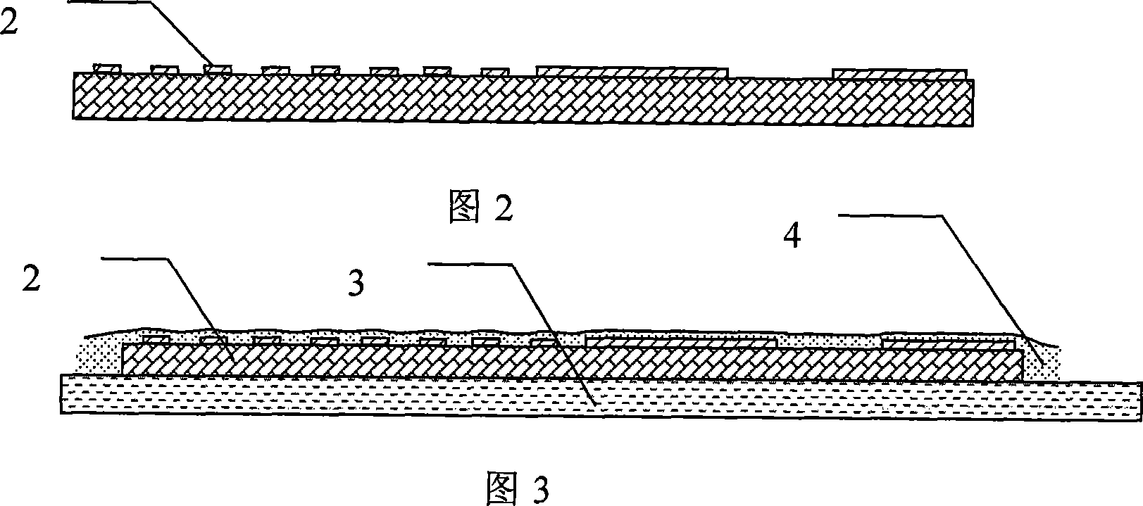
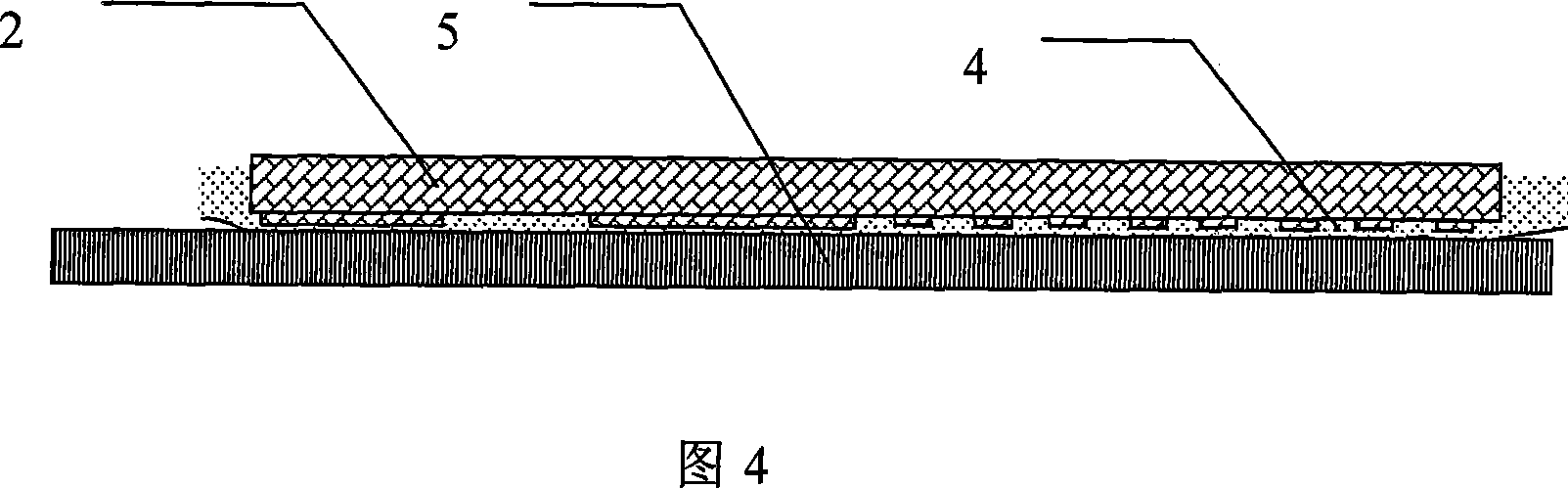
[0037] Embodiment 1, the line structure of the line feature size of 100 nanometers and 20 microns copied by the method of the present invention, as shown in Figures 1, 2, 3, 4, and 5, the production process is as follows:

[0038] (1) First use the existing electron beam direct writing to make a hard template with a micro-nano structure. The line feature sizes are 100nm and 20 microns respectively. Figure 1 is a cross-sectional view of the hard template structure, and 1 represents the material silicon of the hard template;

[0039] (2) Casting the pre-polymerized PDMS material on the surface of the hard template to form a soft PDMS template, the section is as shown in Figure 2, and 2 represents the material PDMS of the soft template;

[0040] (3) Adhering the non-graphic surface of the soft template to the substrate surface 3 through double-sided polishing;

[0041](4) Place the substrate 3 adhered with the soft template on the suction cup of the glue spinner, drop the photore...


PUM


Abstract

A soft pressing method of large-scale micro-nanostructure includes processing out required micronanopattern structure on surface of hard substrate by photo-etching means, coating organic material PDMS on surface of finished hard template, dripping and spiral-coating organic slushing compound on surface of substrate, contacting structure surface of said template closely with polished surface of substrate, picking said template up from said substrate to leave micronanostructure of organic slushing compound on surface of said substrate and using dry means of etching process to remove off base resin or to transfer micronanopattern to surface of said substrate.

Description

technical field [0001] The invention relates to a new method for realizing the formation of large-area micro-nano structures by using a soft mold embossing method. Background technique [0002] In recent years, with the rapid development of micro-nano processing technology and nanomaterials, the formation and pattern transfer of micro-nano structures are receiving more and more attention. In February 2003, Technology Review reported that one of the top ten emerging technologies that will change the world is Nanoimprint Lithography. Such a concept of nano transfer printing technology can be said to be derived from the behavior of stamping in daily life: that is, to imprint the stamp with ink pad on the surface of a flat object with ink pad. This action transfers the pattern originally on the stamp to the surface of another object. [0003] Nanoimprint technology is an idea proposed by Professor S.Y.Chou of Princeton University in the United States in 1996, mainly for the de...

Claims


Application Information

Patent Timeline
IPC IPC(8): G03F7/00
Inventor 董小春杜春雷史立芳罗先刚
Owner INST OF OPTICS & ELECTRONICS - CHINESE ACAD OF SCI
Why Eureka
Try Eureka