

Circuit structure of organic thin film transistor with dual-gate and its use
A thin-film transistor and organic thin-film technology, which is applied in the field of circuit structures with dual-gate organic thin-film transistors, can solve the problems of high starting voltage, malfunction of switch components in pixel areas, signal transmission distortion, etc., and achieves the effect of a simple structure
- Summary
- Abstract
- Description
- Claims
- Application Information
AI Technical Summary
Problems solved by technology
Method used
Image

Examples
Embodiment Construction
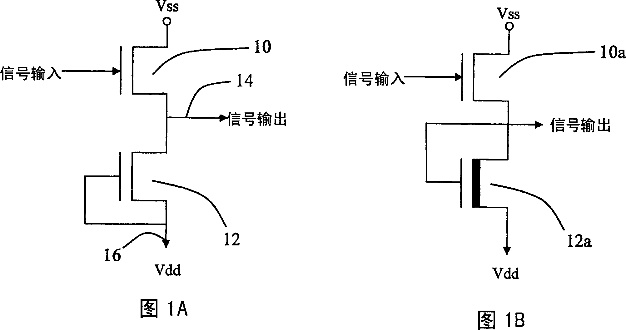
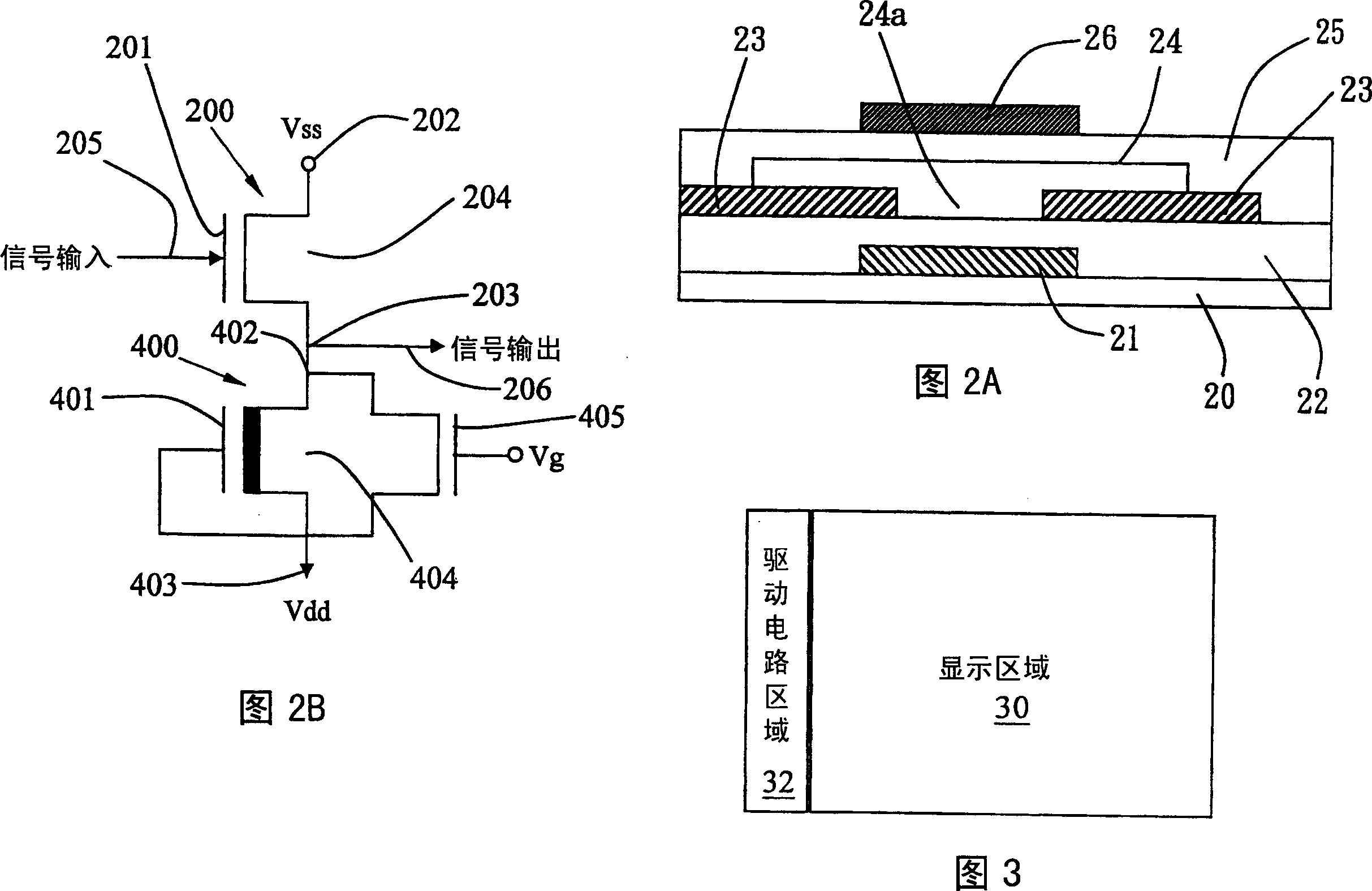
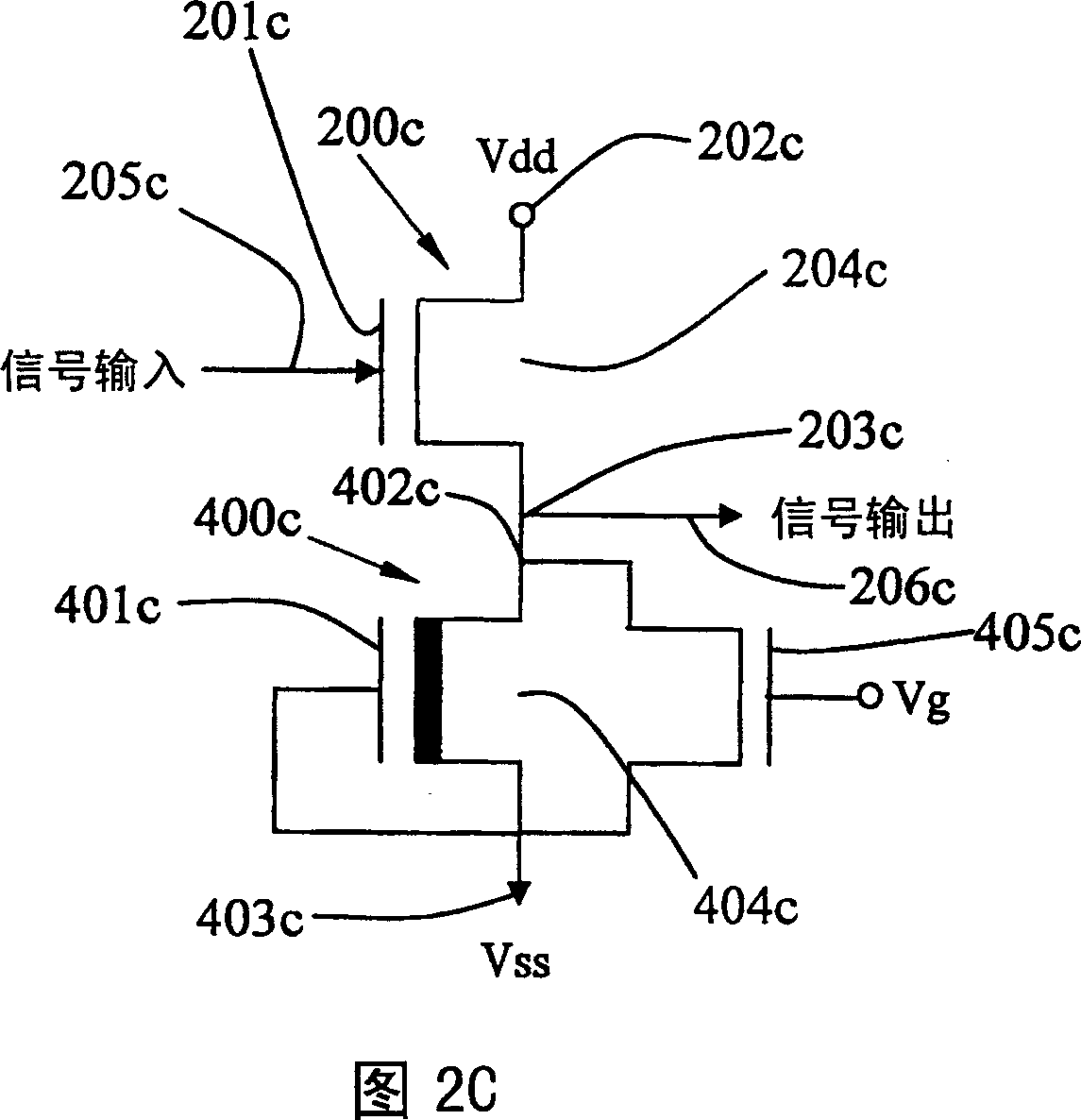
[0047]In the present invention, a protective layer is covered on the organic thin film transistor structure with a bottom gate, and the protective layer is used as another gate insulating layer, and another metal layer is partially formed on the protective layer to make as another gate to complete an organic thin film transistor structure with double gates. In the organic thin film transistor structure with double gates, the aforementioned double gates share a pair of source and drain and an organic semiconductor channel region (organicsemiconductor channel), and the starting voltage of the organic thin film transistor is the first gate voltage of the organic thin film transistor. The sum of the starting voltage of the organic thin film transistor and the second gate, so the starting voltage of the organic thin film transistor can be adjusted and lowered through its double gate structure. Furthermore, the organic thin film transistor can be controlled to operate as a depletion...
PUM
 Abstract
Description
Claims
Application Information