Check patentability & draft patents in minutes with Patsnap Eureka AI!

Method for producing non-volatile memory

A manufacturing method and non-volatile technology, applied in semiconductor/solid-state device manufacturing, electrical components, circuits, etc., can solve problems such as increasing the difficulty of lithography process, achieve process margin and reliability improvement, and uniform gate coupling efficiency, process simplification

Active Publication Date: 2007-11-21
MACRONIX INT CO LTD
View PDF0 Cites 0 Cited by
  • Summary
  • Abstract
  • Description
  • Claims
  • Application Information

AI Technical Summary

Problems solved by technology

The invention provides a manufacturing method of a non-volatile memory, which can increase the gate coupling rate and improve the device performance. In addition, the method avoids increasing the difficulty of the lithography process, and alleviates the bridging phenomenon and the gate coupling rate due to the difficulty of the process. the problem of change

Method used


Image

  • Method for producing non-volatile memory
  • Method for producing non-volatile memory
  • Method for producing non-volatile memory

Examples


Embodiment Construction

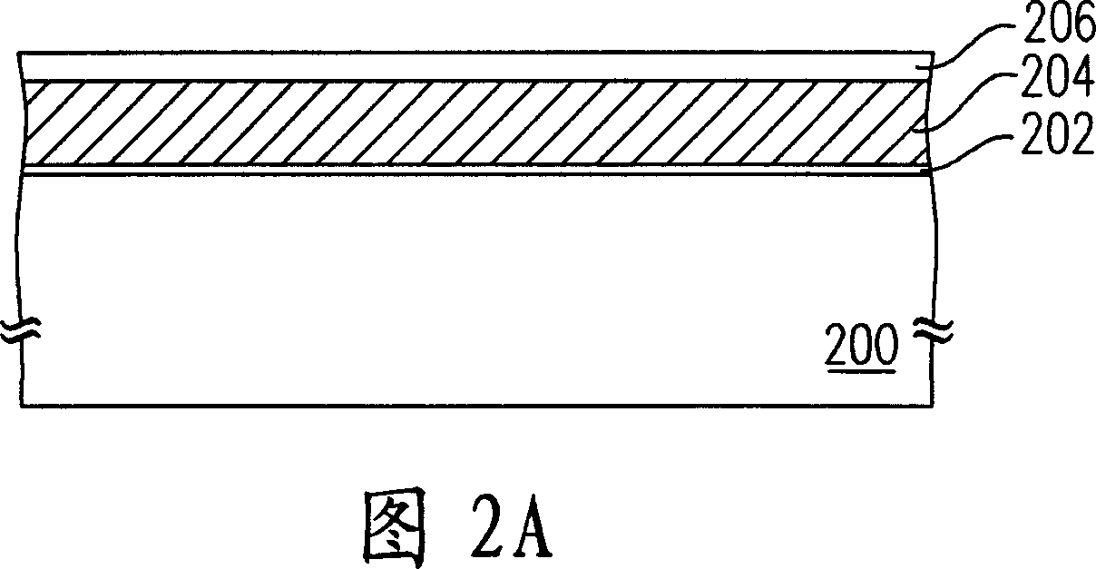
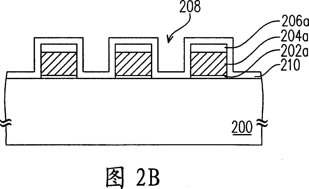
[0026] 2A to 2E are cross-sectional views of the manufacturing process of the non-volatile memory according to an embodiment of the present invention.

[0027] First, please refer to FIG. 2A , a substrate 200 is provided. The material of the substrate 200 is silicon, for example. A first dielectric layer 202 is formed on the substrate 200 . The first dielectric layer 202 is, for example, a tunnel oxide layer, and the formation method of the first dielectric layer 202 is, for example, a thermal oxidation method. A conductive layer 204 is formed on the first dielectric layer 202 . The material of the conductive layer 204 is, for example, doped polysilicon, and the formation method of the conductive layer 204 is, for example, a chemical vapor deposition process of on-site doping. Next, a mask layer 206 is formed on the conductive layer 204 . The material of the mask layer 206 is, for example, silicon nitride, and the method of forming the mask layer 206 is, for example, chemi...


PUM

PropertyMeasurementUnit
Thicknessaaaaaaaaaa
Thicknessaaaaaaaaaa
Thicknessaaaaaaaaaa

Abstract

This is a production method for a non-volatile memory unit. A layer of dielectric layer, the premier conducting layer and the masking layer are formed in order on the base with floating gate and multi-patches. Interval walls are formed on the patch side walls. The source electrodes are formed on the base under the patches. Oxidize the base under the patches to form an insulation layer. Then remove the masking layer and forms another dielectric layer on the conducting layer and insulation layer. The secondary conducting layer is then formed on the secondary dielectric layer.

Description

technical field [0001] The present invention relates to a manufacturing method of a semiconductor element, and in particular to a manufacturing method of a non-volatile memory. Background technique [0002] In the non-volatile memory, data can be stored, read, and erased multiple times, and the stored data will not disappear after power failure, and it has fast access speed and light weight Due to the advantages of large capacity and small size of the access device, it has become a memory component widely used in personal computers and electronic equipment. [0003] A typical non-volatile memory device is generally designed to have a stack-gate (Stack-Gate) structure, which includes doped polysilicon to make a floating gate (Floating Gate) and a control gate (Control Gate). The floating gate is located between the control gate and the substrate, and is in a floating state, not connected to any circuit, while the control gate is connected to the word line (Word Line), and al...

Claims


Application Information

Patent Timeline
IPC IPC(8): H01L21/336H01L21/8247
Inventor 林新富吴俊沛
Owner MACRONIX INT CO LTD
Features
  • R&D
  • Intellectual Property
  • Life Sciences
  • Materials
  • Tech Scout
  • Unparalleled Data Quality
  • Higher Quality Content
  • 60% Fewer Hallucinations
Learn More