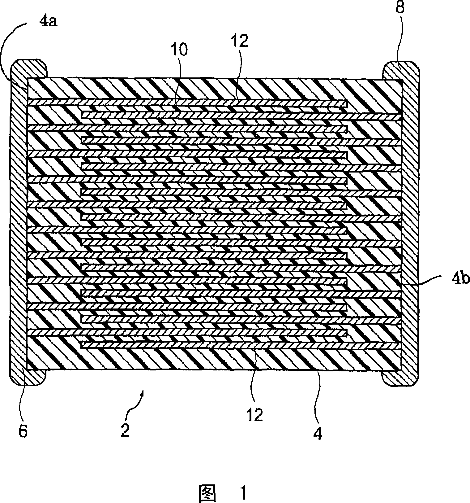
Electronic component, multilayer ceramic capacitor, and method for fabricating same
A technology of ceramic capacitors and electronic components, which is applied in the direction of multilayer capacitors, capacitors, fixed capacitors, etc., can solve the problem of difficulty in continuously forming electrode layers, difficulty in miniaturization and large capacity of multilayer ceramic capacitors, and the electrostatic capacity of multilayer ceramic capacitors. Easy to reduce and other problems, to achieve the effect of suppressing the reduction of electrostatic capacity
- Summary
- Abstract
- Description
- Claims
- Application Information
AI Technical Summary
Problems solved by technology
Method used
Image
Examples
Embodiment 1
[0127] Preparation of each paste
[0128] First, the BaTiO 3 Powder (BT-02 / Sakai Chemical Industry Co., Ltd.) and MgCO 3 , MnCO 3 , (Ba 0.6 Ca 0.4) SiO 3 And selected from rare earths (Gd 2 o 3 , Tb 4 o 7 、Dy 2 o 3 、Ho 2 o 3 、Er 2 o 3 、Tm 2 o 3 , Yb 2 o 3 、Lu 2 o 3 , Y 2 o 3 ) powder was wet-mixed by ball milling for 16 hours, and then dried to make a dielectric material. The average particle diameter of these raw material powders is 0.1-1 μm. (Ba 0.6 Ca 0.4 ) SiO 3 is the BaCO 3 , CaCO 3 and SiO 2 It was wet-mixed by ball milling for 16 hours, dried and sintered in air at 1150° C., and then wet pulverized by ball milling for 100 hours.
[0129] In order to form the obtained dielectric material into a paste, the organic vehicle was added to the dielectric material and mixed by a ball mill to obtain a paste for dielectric green sheets. The organic vehicle is, relative to 100 parts by mass of the dielectric material, polyvinyl butyral as a binder: ...
Embodiment 2
[0181] The dielectric green sheet paste prepared in Example 1 was coated on a PET film (carrier sheet) using a wire bar coater, and then dried to obtain a green sheet 10a. The same procedure as in Example 1 was carried out. In this method, a pre-sintered internal electrode thin film 12a is formed on the green sheet 10a to prepare a laminate as shown in FIG. 8 . Next, the PET film was peeled off from the laminate to prepare a pre-sintered sample composed of the green sheet 10a and the internal electrode film 12a, and the pre-sintered sample was subjected to binder removal, sintering, and sintering in the same manner as in Example 1. Annealing is performed to prepare a sample for surface observation after sintering including the dielectric layer 10 and the internal electrode layer 12 .
[0182] Next, the obtained sample for surface observation was observed by SEM from a direction perpendicular to the surface on which the internal electrode layer 12 was formed, and the internal e...
Embodiment 3
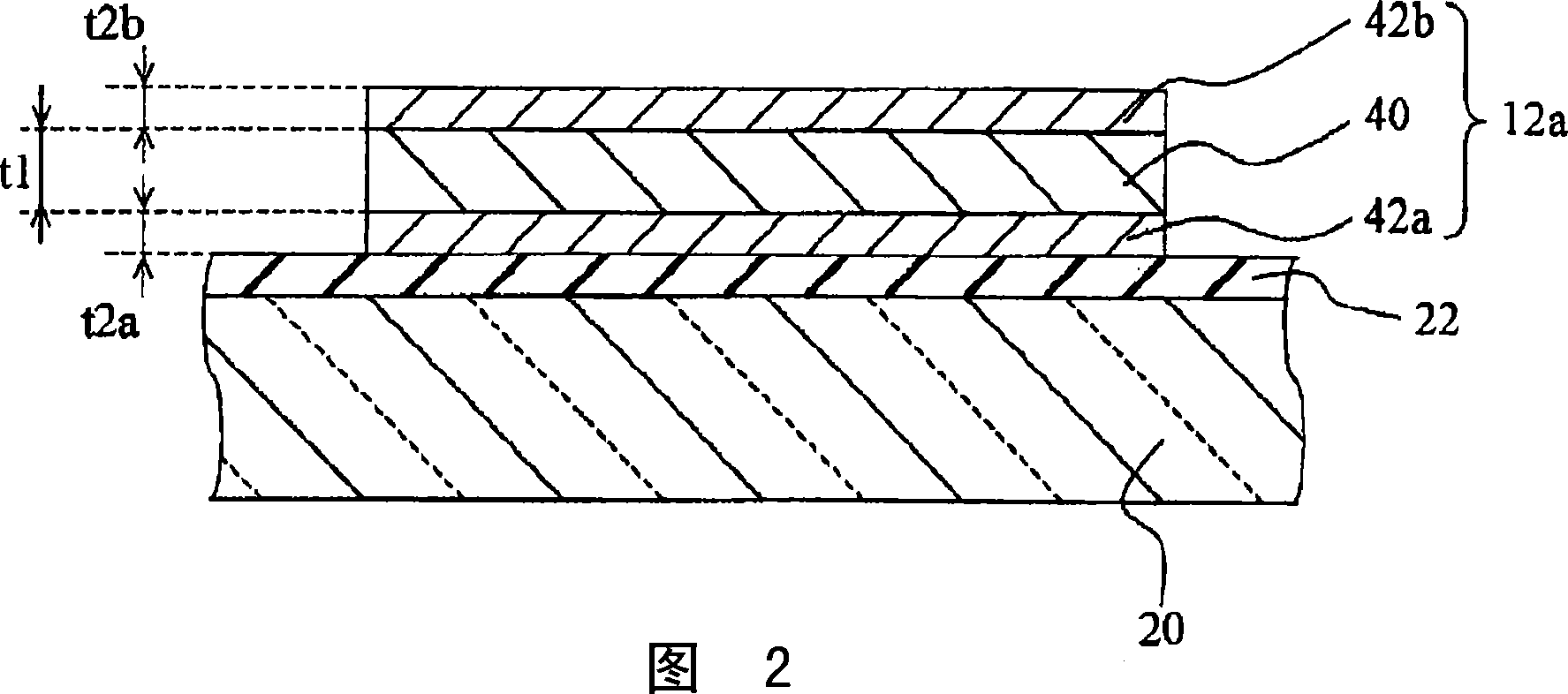
[0186] MgO, Al 2 o 3 , SiO 2 , CaO, TiO 2 , V 2 o 3 , MnO, SrO, Y 2 o 3 , ZrO 2 , Nb 2 o 5 , BaO, HfO 2 , La 2 o 3 、Gd 2 o 3 , Tb 4 o 7 、Dy 2 o 3 、Ho 2 o 3 、Er 2 o 3 、Tm 2 o 3 , Yb 2 o 3 、Lu 2 o 3 , CaTiO 3 or SrTiO 3 instead of BaTiO 3 , except that the sample was obtained in the same manner as in Example 1. The thickness t1 of the metal thin film 40 of each of the above-mentioned samples is 0.4 μm, and the thicknesses t2a and t2b of the dielectric thin films 42a and 42b are respectively 0.05 μm, that is, the total thickness t2 (t2=t2a+t2b) of the dielectric thin films 42a and 42b is 0.1 μm. . The electrical characteristics (capacitance C, dielectric loss tan δ) of each sample were evaluated in the same manner as in Example 1. The results are shown in Table 2.
[0187]
sample
dielectric thin
film 42a,
Group 42b
become
Metal film 40
Thickness t1[μm]
Dielect...
PUM
| Property | Measurement | Unit |
|---|---|---|
| particle size | aaaaa | aaaaa |
| thickness | aaaaa | aaaaa |
| thickness | aaaaa | aaaaa |
Abstract
Description
Claims
Application Information


