

FEOL/MEOL metal resistor for high end CMOS
A technology of resistors and metals, applied in the field of complementary metal oxide semiconductors, can solve problems such as low parasitic capacitance
- Summary
- Abstract
- Description
- Claims
- Application Information
AI Technical Summary
Problems solved by technology
Method used
Image

Examples
no. 1 example
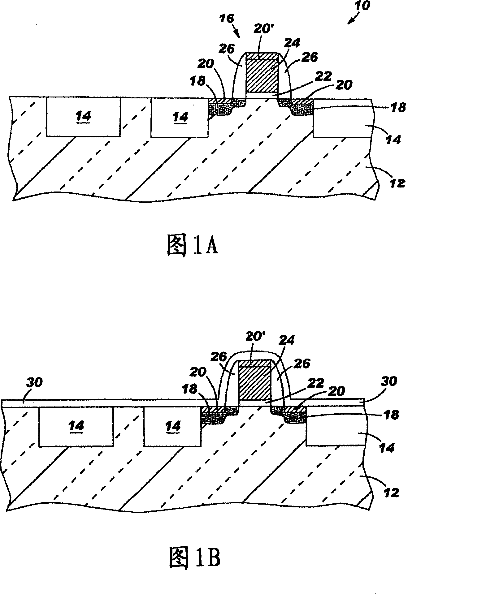
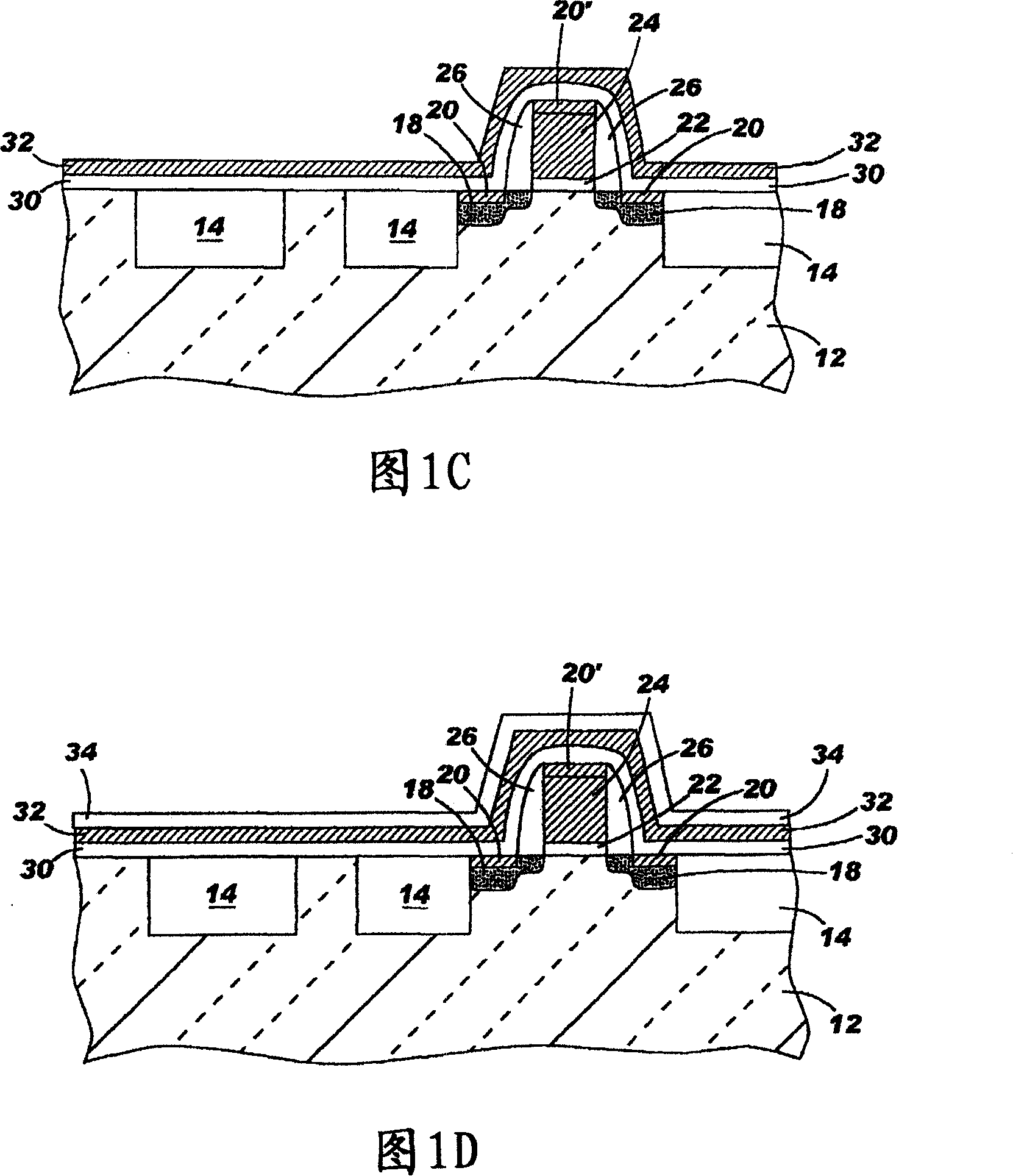
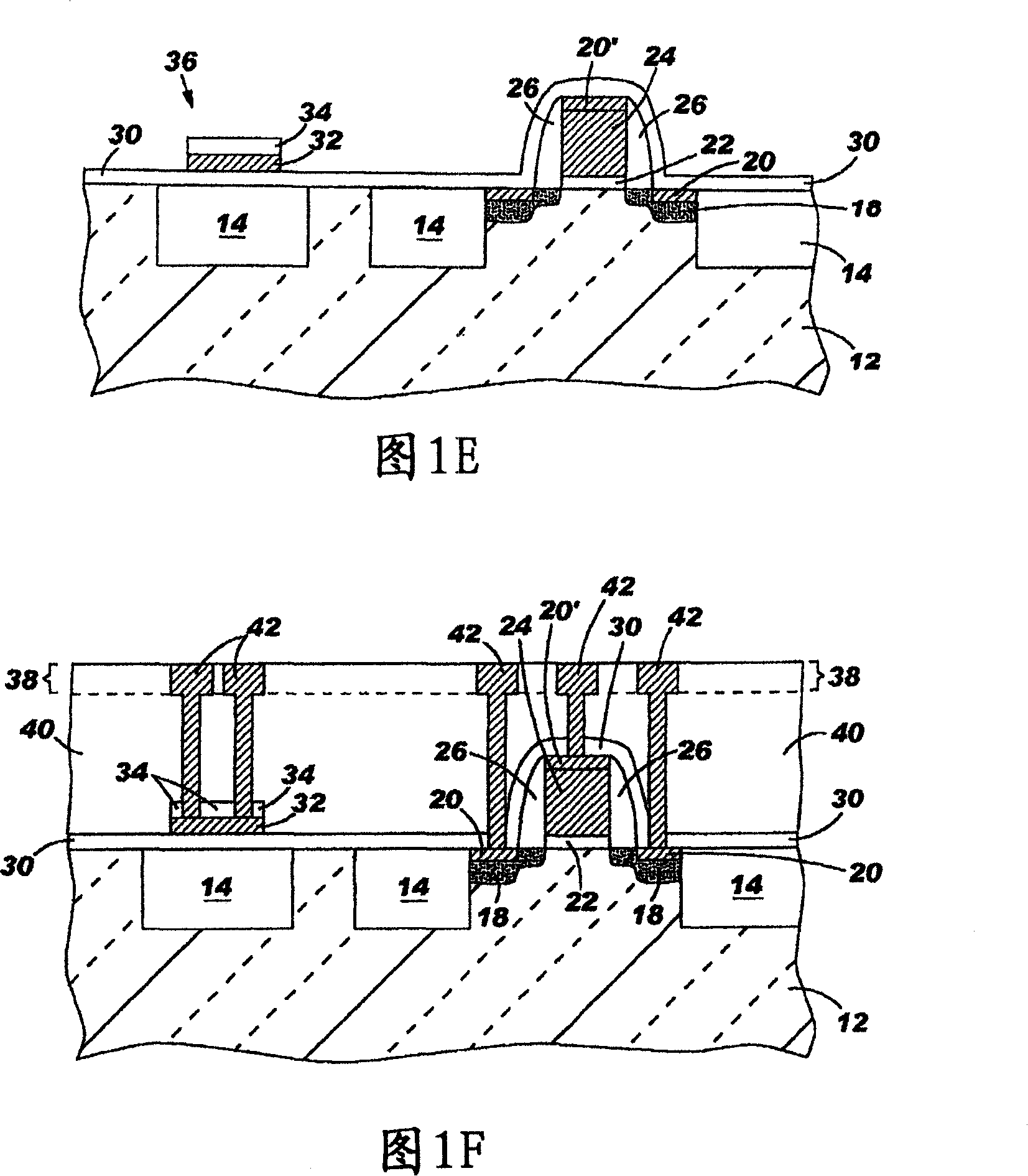
[0043] First Embodiment: Reference is first made to the embodiment described in Figures 1A-1F. This embodiment initially provides the structure 10 shown in Figure 1A. Structure 10 includes a processed semiconductor substrate 12 including at least one trench isolation region 14 in semiconductor substrate 12 , and at least one FEOL device 16 on a surface of semiconductor substrate 12 . In this figure, at least one FEOL device 16 is a field effect transistor (FET) comprising a source / drain region 18, a silicide region 20 atop the source / drain region 18, a gate dielectric 22, A gate conductor 24 , an optional silicide region 20 ′ on gate conductor 24 , and at least one spacer 26 on at least a sidewall of gate conductor 24 . Although FETs are illustrated as FEOL devices, the present invention also contemplates other types of FEOL devices including, for example, bipolar transistors, BiCMOS devices, passive devices, and any other similar devices formed in the front end of processing...
no. 2 example
[0062] Second Embodiment: Referring to the structure 50 shown in FIG. 2A, which includes the semiconductor substrate 12, the trench isolation region 14, and the FEOL devices 16 and 16'. FEOL device 16 is a FET and FEOL device 16' is a bipolar device. For clarity, FEOL devices 16 and 16' are shown as a single box in the drawings of the present invention. The structure shown in FIG. 2A is formed using the techniques described in the first embodiment for FIG. 1A.
[0063] Next, a planarizing dielectric material 52 is formed, which may be, for example, an oxide of boron-doped silicate glass or another ILD-like material (see first embodiment above). The planarizing dielectric material 52 is formed by conventional deposition processes, and if desired, a planarizing process such as chemical mechanical polishing (CMP) or grinding may be used. The resulting structure comprising planarized dielectric material 52 is shown in FIG. 2B . Planarizing dielectric material 52 has a thickness...
no. 3 example
[0068] Third Embodiment: This embodiment differs from the previous embodiments in that the resistors comprise metal silicides, which are formed during silicidation of the FEOL device. A third embodiment of the invention begins by providing the structure 60 shown in Figure 3A. This structure includes at least one FEOL device 16 including at least one trench isolation region 14 on the surface of a semiconductor substrate 12 . The shown and illustrated FEOL device 16 is a FET that still does not contain any silicide regions. Although FET devices are shown, the third embodiment can work with other FEOL devices that include silicide regions.
[0069] Next, a suicide metal layer 62 is formed over the structure, providing the structure shown in FIG. 3B. The suicide metal 62 used in this embodiment of the invention includes any metal capable of reacting with silicon to form a metal suicide. Examples of such metals include, but are not limited to: Ti, Ta, W, Co, Ni, Pt, Pd and alloy...
PUM
 Abstract
Description
Claims
Application Information