Implementing method for interconnected structure of RF MEMS switch

A technology of interconnection structure and realization method, which is applied in the direction of circuits, waveguide devices, electrical components, etc., can solve the problems of reducing the reliability of switches, complicated switch processing technology, warping and deformation of switch structures, etc., and achieves the improvement of mechanical strength and reliability , The method and structure are simple and practical, and the effect of avoiding warping and deformation

Inactive Publication Date: 2007-12-19
PEKING UNIV
View PDF0 Cites 10 Cited by
  • Summary
  • Abstract
  • Description
  • Claims
  • Application Information

AI Technical Summary

Problems solved by technology

[0005] 1) The stress of the silicon nitride film will warp and deform the switch structure, and even cause the switch to fail;
[0006] 2) The adhesion between the silicon nitride film and the structural material polysilicon is poor, it is easy to fall off, and cannot withstand high mechanical force; thus affecting the stability of the switch contact and reducing the reliability of the switch
[0007] The difficulty in the design of the interconnection structure complicates the switch processing technology and increases the cost. At the same time, it reduces the working performance and reliability of the switch, which seriously affects the application prospect and market competitiveness of the switch.

Method used


Image

  • Implementing method for interconnected structure of RF MEMS switch
  • Implementing method for interconnected structure of RF MEMS switch
  • Implementing method for interconnected structure of RF MEMS switch

Examples


example 1

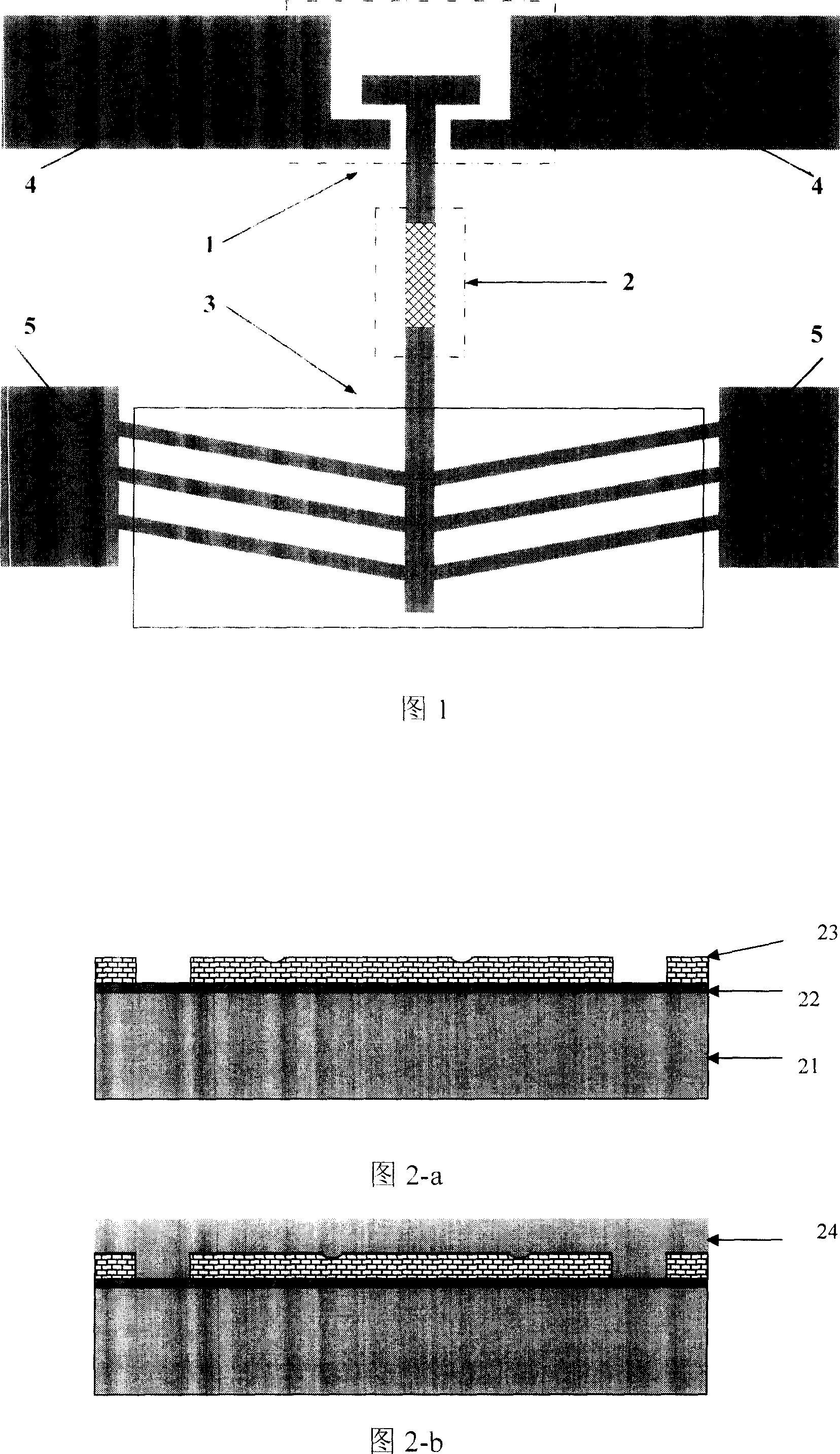
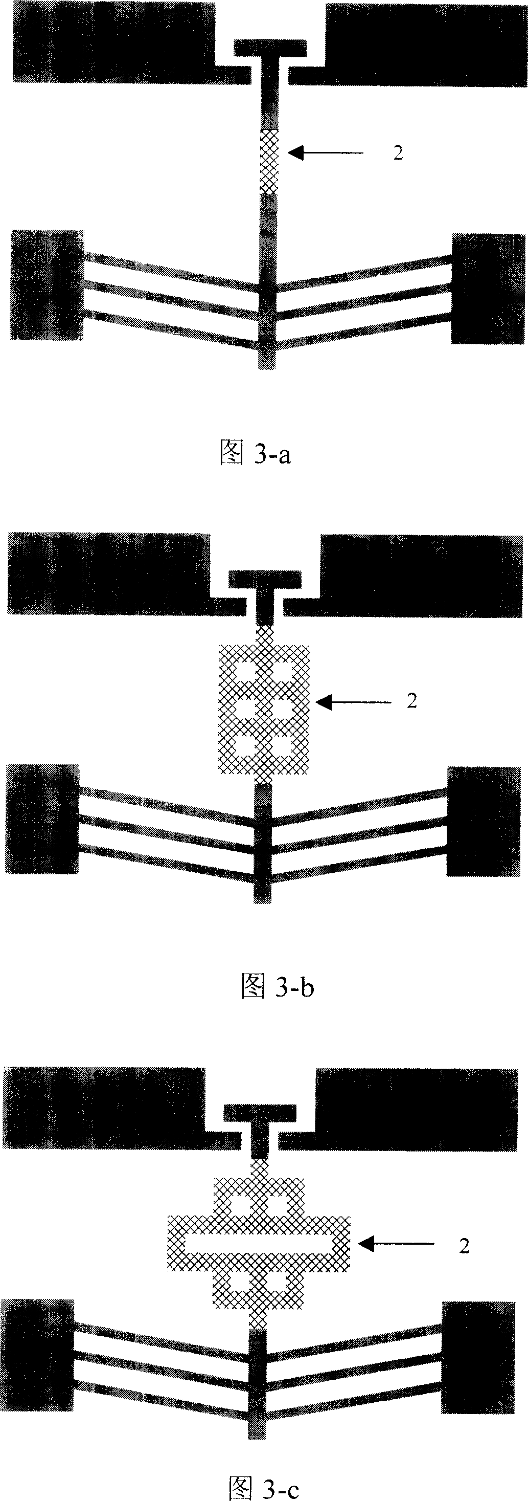
[0047] The schematic diagram of the planar structure of the interconnection structure is shown in Fig. 1 . Structures 1, 2, and 3 are drive structures, interconnect structures, and contact structures, respectively, and structures 4 and 5 are signal lines and anchor points, respectively. The entire switch structure is formed by one polysilicon deposition with a thickness of 2um.

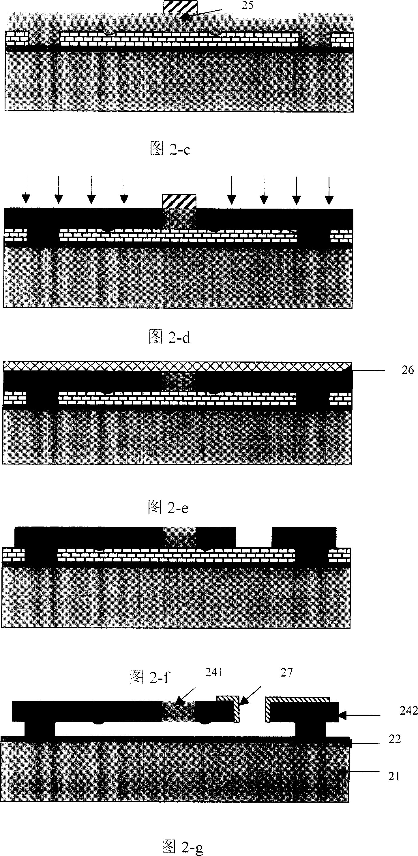
[0048] Referring to Figure 2, the process flow of the switch is as follows:

[0049] 1) An N Si sheet is selected as the Si substrate 21 with a thickness of 400um and a diameter of 4 inches. A silicon nitride insulating layer 22 is deposited by LPCVD to a thickness of 1000 angstroms. A SiO2 sacrificial layer 23 is deposited by LPCVD with a thickness of 2um. Photolithography, and use RIE etching to pattern the sacrificial layer structure;

[0050] 2) Deposit polysilicon 24 with a thickness of 2um by LPCVD;

[0051] 3) Spin the glue and perform photolithography, using the remaining photoresist afte...

example 2

[0057] The schematic diagram of the planar structure of the interconnection structure is shown in Fig. 1 . Structures 1, 2, and 3 are drive structures, interconnect structures, and contact structures, respectively, and structures 4 and 5 are signal lines and anchor points, respectively. The thickness of the whole switch structure is 4um.

[0058] The process flow of the switch is as follows:

[0059] 1) Select N Si sheet as the Si substrate, with a thickness of 400um and a diameter of 4 inches. A silicon nitride insulating layer is deposited by LPCVD to a thickness of 500 angstroms. The SiO2 sacrificial layer is deposited by LPCVD method with a thickness of 2um. Photolithography, and use RIE etching to pattern the sacrificial layer structure;

[0060] 2) Deposit polysilicon with a thickness of 4um by LPCVD method;

[0061] 3) Deposit SiO2 with a thickness of 2um as a mask layer by LPCVD method, and use photolithography and RIE etching to pattern the SiO2 film;

[0062] 4) ...


PUM


Abstract

This invention provides a realizing method for interlinking structure of RF MEMS switch, which utilizes generation of primary polysilicon to prepare a drive, interlinking structure and a contact part of the RF MEMS switch, in which, the drive and contact parts are doped polysilicon and the interlinking structure between them is non-doped. The invention takes non-doped polysilicon as the interlinking structure between the drive structure and the contact part of the RF MEMS switch to get the result of electric insulation effectively at the time realizing mechanical interlinking.

Description

technical field [0001] The invention belongs to the technical field of radio frequency micro-electromechanical switches (RF MEMS Switches), and in particular relates to a method for realizing an interconnection structure of RF MEMS switches. Background technique [0002] As a switch structure that has emerged in recent years and has gradually received attention, RF MEMS Switch has the advantages of low insertion loss and can be integrated with IC circuits, and meets the development needs of high-frequency and miniaturization of wireless communication technology. Broad application prospects. As wireless communication (Wireless Communication) technology enters the radio frequency scale, radio frequency MEMS switches have gradually replaced traditional GaAsFET switches and become the development direction of radio frequency switches (RF Switch). [0003] In recent years, various RF MEMS switch structures have been developed. Among them, the lateral switch (Lateral Switch) rea...

Claims


Application Information

Patent Timeline
Patent Type & Authority Applications(China)
IPC IPC(8): H01P1/12
Inventor 李志宏施文典
Owner PEKING UNIV
Why Eureka
Try Eureka