Radio frequency metal-oxide semiconductor device, and manufacturing method

A technology of oxide semiconductor and manufacturing method, which is applied in semiconductor/solid-state device manufacturing, semiconductor device, semiconductor/solid-state device components and other directions, can solve the problems of reducing device performance such as the lowest noise figure of gain, etc., to reduce noise, reduce The effect of parasitic resistance

Inactive Publication Date: 2007-12-26
SEMICON MFG INT (SHANGHAI) CORP
View PDF1 Cites 4 Cited by
  • Summary
  • Abstract
  • Description
  • Claims
  • Application Information

AI Technical Summary

Problems solved by technology

However, the noise generated by the alternating magnetic field generated by the high-frequency current in the upper interconnection metal layer coupled in the MOS device is still not resolved, and the noise will still reduce the performance of the device such as gain, minimum noise figure, etc.

Method used


Image

  • Radio frequency metal-oxide semiconductor device, and manufacturing method
  • Radio frequency metal-oxide semiconductor device, and manufacturing method
  • Radio frequency metal-oxide semiconductor device, and manufacturing method

Examples


Embodiment Construction

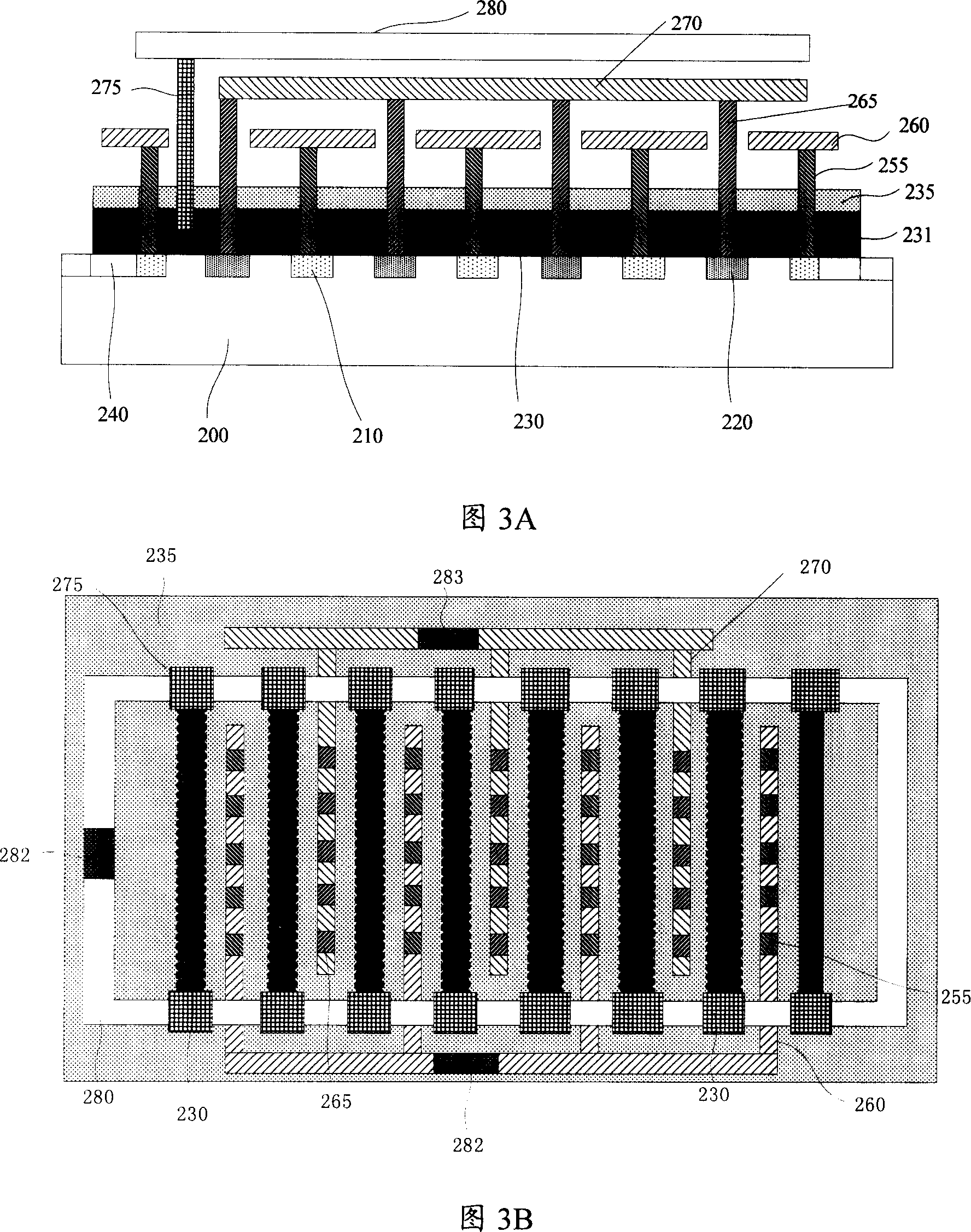
[0043] The specific embodiments of the present invention will be described in detail below in conjunction with the accompanying drawings.

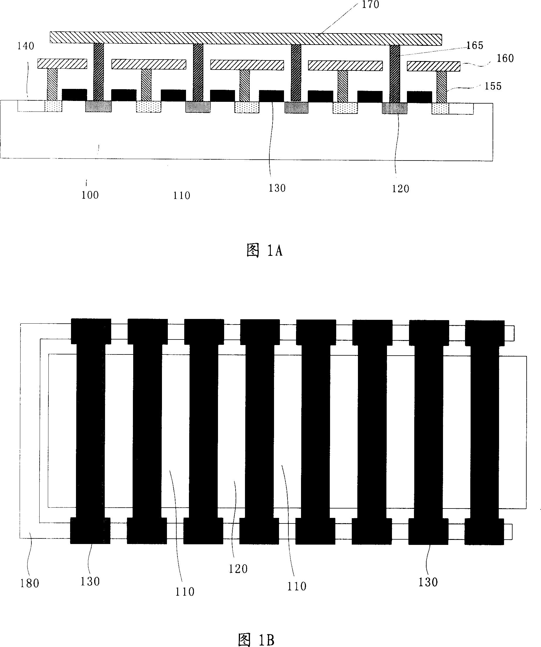
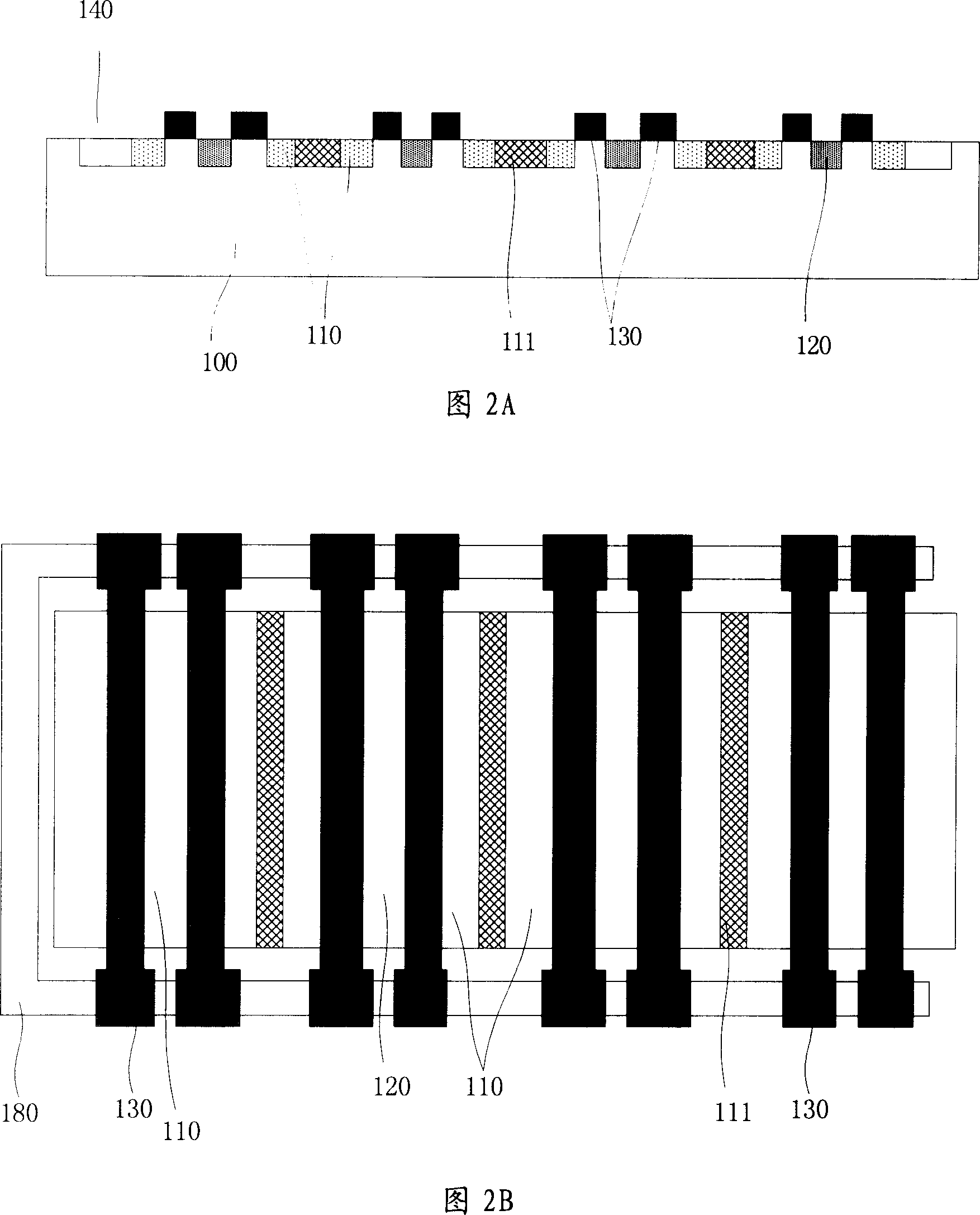
[0044]3A and 3B are structural diagrams of the radio frequency metal oxide semiconductor device according to the first embodiment of the present invention. As shown in FIG. 3A , a complex gate radio frequency metal oxide semiconductor transistor (MOSFET) is formed on a semiconductor substrate 200 . The source 210 and the drain 220 of the complex-gate RF metal-oxide-semiconductor transistor are arranged in sequence. A gate 230 is formed on the substrate between the source 210 and the drain 220 , the thickness of the gate oxide is 1.0 nm˜4.0 nm, and the thickness of the polysilicon is 200 nm. The gate width is 65-350nm, and the number of gates is 16 or 32, arranged in parallel with each other. The use of a complex gate structure can reduce the gate resistance and reduce the parasitic resistance formed between the gate channel and the sourc...


PUM


Abstract

The device includes following parts: a semiconductor substrate; a device layer formed on the semiconductor substrate; a shielding layer formed on the device layer; and an interconnection layer formed on the shielding layer. The manufacturing method includes steps: providing a semiconductor substrate; forming a device layer on the semiconductor substrate; forming an insulating layer on the device layer; forming a shielding layer on the insulating layer; forming connection holes between the shielding layer and the insulating layer; forming an interconnection layer on the shielding layer. The shielding layer shields influence on transistor from electromagnetic radiation generated by the interconnection layer, and makes testing semiconductor device simple, and accurate.

Description

technical field [0001] The invention relates to the technical field of semiconductor manufacturing, in particular to a radio frequency metal oxide semiconductor device and a manufacturing method thereof. Background technique [0002] Silicon-based radio frequency metal oxide semiconductor devices have been widely used in the field of wireless communication. With the continuous advancement of manufacturing technology, the size of devices is getting smaller and smaller, and higher requirements are put forward for indicators such as device impedance matching, high-frequency gain, and radio frequency noise figure. Due to continuous work, the device continues to age, the function gradually declines, the stability deteriorates, and the gain and minimum RF noise figure and other indicators will also deteriorate with the increase of the operating frequency. In particular, the current ultra-wide band (Ultra-wide band) wireless communication technology requires a very high operating ...

Claims


Application Information

Patent Timeline
Patent Type & Authority Applications(China)
IPC IPC(8): H01L27/04H01L23/552H01L23/522H01L21/822H01L21/768
CPCH01L2924/0002
Inventor 廖金昌黄威森张莉菲
Owner SEMICON MFG INT (SHANGHAI) CORP
Why Eureka
Try Eureka