A short-wavelength algainp red semiconductor laser
A semiconductor and laser technology, applied in the field of red light semiconductor lasers, can solve the problems of low efficiency and low strain of semiconductor lasers, and achieve the effects of improving electro-optical conversion efficiency, improving growth quality, and reducing heat generation.
- Summary
- Abstract
- Description
- Claims
- Application Information
AI Technical Summary
Problems solved by technology
Method used
Image
Examples
Embodiment Construction
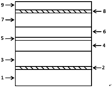
[0027] like figure 1 As shown, the short-wavelength AlGaInP red semiconductor laser of the present invention has a structure from bottom to top successively as substrate 1, lower buffer layer 2, lower confinement layer 3, lower waveguide layer 4, quantum well layer 5, upper waveguide layer 6, Upper confinement layer 7 , upper buffer layer 8 and ohmic contact layer 9 .
[0028] The substrate 1 is common N-type GaAs.
[0029] The lower buffer layer 2 is Al with a thickness of 1-2 μm x In 1-x P, Al composition x linearly changes from 0.5 to 0.6, that is, the first layer of growth is Al that matches the GaAs lattice 0.5 In 0.5 P, the last layer is Al 0.6 In 0.4 P, and the last layer of lattice strain is released, and its lattice constant is the same as that of the bulk material Al 0.6 In 0.4 p.
[0030] The lower confinement layer 3 and the upper confinement layer 7 are both 2-3 μm thick Al 0.6 In 0.4 p. For 620nm red wavelength, Al 0.6 In 0.4 The refractive index of...
PUM
 Abstract
Description
Claims
Application Information
