LED chip surface fluorescent powder layer coating method

A technology of LED chip and coating method, which is applied to the device and coating of the surface coating liquid, which can solve the problems of uneven wavelength conversion, light and color shift of LED components, and inability to commercialize mass production.

Inactive Publication Date: 2008-01-09
INTEX OPTOELECTRONICS XIAMEN CO LTD
View PDF0 Cites 25 Cited by
  • Summary
  • Abstract
  • Description
  • Claims
  • Application Information

AI Technical Summary

Problems solved by technology

The second is three-chip three-primary colors (blue light + green light + red light) mixed into white light, but circuit control is required to obtain a stable color, and the cost is relatively high
The third is the three-wavelength light that is more promising in the future, especially the combination of red, green and blue three-color phosphors on the ultraviolet chip. mass production
The dispensing method of the dispensing machine is to use gravity to let the silica gel or epoxy resin containing the phosphor flow and then cover the LED chip. Therefore, the thickness of the phosphor cannot be fully averaged on the LED light-emitting surface, which will cause wavelength conversion. Uniformity, causing problems such as light color shift and uneven light color of LED components

Method used


Image

  • LED chip surface fluorescent powder layer coating method
  • LED chip surface fluorescent powder layer coating method
  • LED chip surface fluorescent powder layer coating method

Examples


Embodiment approach 1

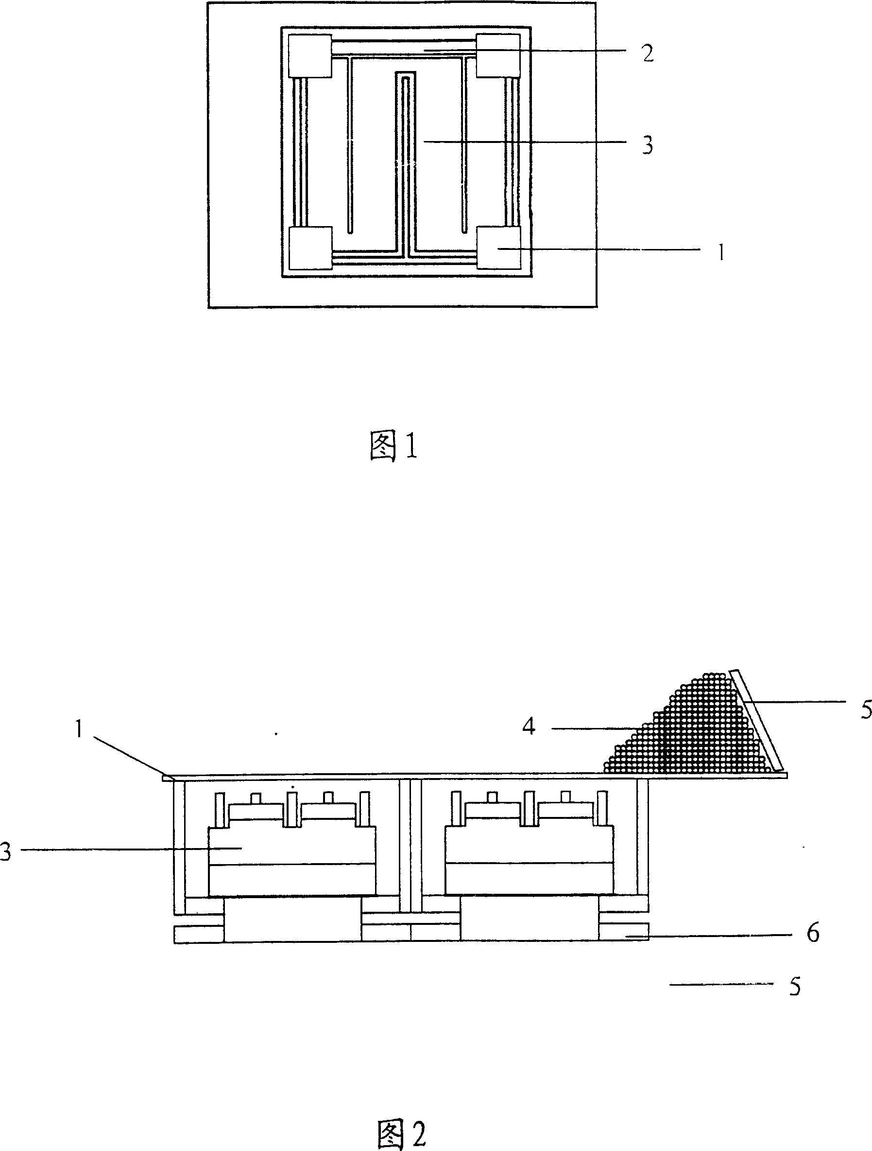
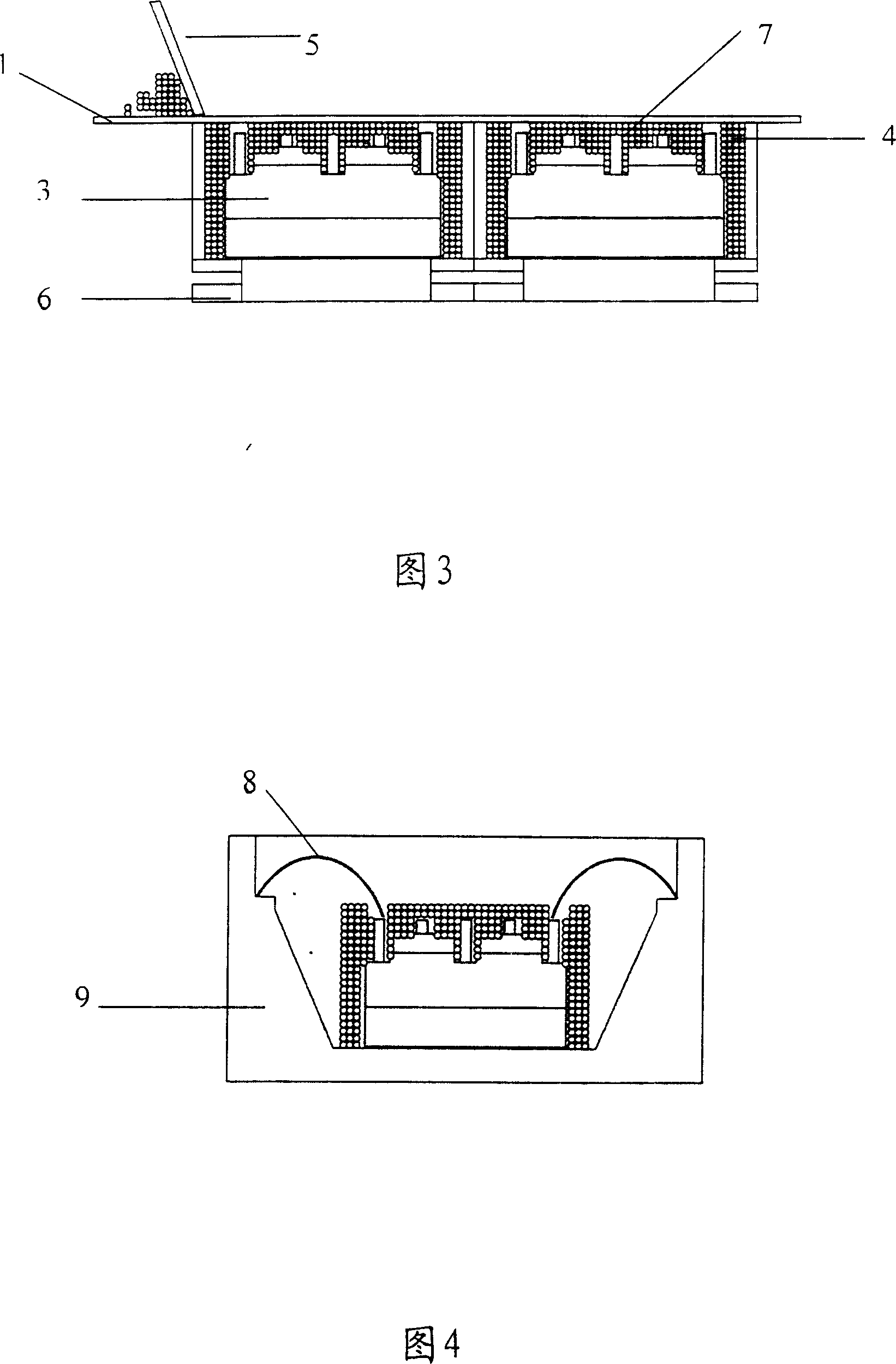
[0026] Implementation method 1: as shown in Figure 2 to Figure 4, first separate the divided LED chips 3 (LED chips can be binary materials such as GaN or quaternary materials such as AlGaNP and other various LED chip materials) one by one. Put it on the special fixture 6 or on the metal foil or other carrier or tool. The metal foil can be metal or alloy such as gold, silver, copper and aluminum. Place the screen plate 1 on the jig and open it, then place the pre-mixed fluorescent glue on the plate, use the scraper 5 to push the fluorescent glue back and forth with an appropriate force, so that the fluorescent glue is pushed into the underside of the screen plate. In the gap, fill the space under the fixture, LED chip and screen; as shown in Figure 3, because there is a shielding area on the screen, a vacancy 7 will be formed under the shielding area that is not filled with fluorescent glue , the vacancies can expose the electrodes on the LED chip and not be covered by fluores...

Embodiment approach 2

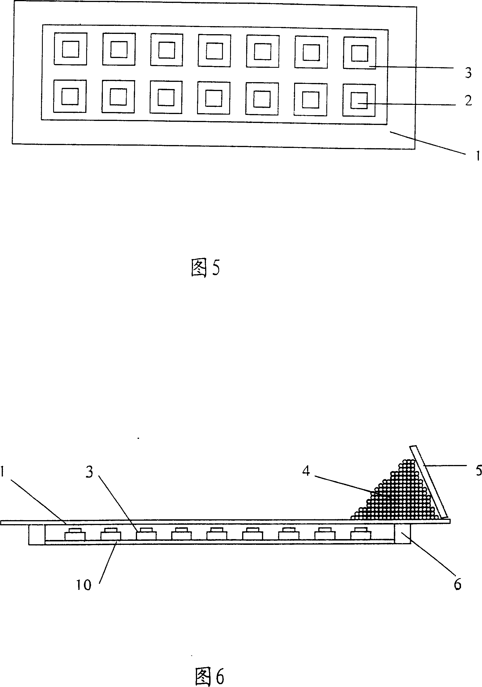
[0027] Implementation method 2: As shown in Fig. 5 to Fig. 8, the shielding area 2 is prepared in advance on the screen plate 1 in Fig. 5 . First fix the LED chip 3 on the copper foil 10 and arrange it well, place the screen plate 1 on the jig 6 and open it, then place the phosphor glue pre-mixed with phosphor powder on the plate, and use the scraper 5 with an appropriate force Push the fluorescent glue back and forth, so that the fluorescent glue is pushed into the gap under the screen, and fills the space under the fixture, LED chips and the screen, as shown in Figure 7, because there is a shielding area on the screen If it exists, a vacancy 7 will be formed under the shielding area and is not filled by the fluorescent glue. The vacancy can expose the electrodes on the LED chip and not be covered by the fluorescent glue. Then use a laser (Laser) or a diamond cutter to cut the LED chips together with fluorescent glue and copper foil into individual pieces, as shown in Figure ...

Embodiment approach 3

[0028] Implementation method three: as shown in Figure 9 to Figure 12, the shielding area 2 is pre-made on the screen plate 1 in Figure 9, and then as shown in Figure 10, the LED chip 11 that has been pre-finished with surface groove treatment is fixed on the clamp Place the screen plate 1 on the jig 6 and open it on the jig 6, then put the fluorescent glue pre-mixed with the phosphor powder on the plate, and push the fluorescent glue back and forth with a proper force with the scraper 5, so that the fluorescent glue is pushed Squeeze into the gap below the screen, and fill the space under the fixture, LED chip and screen, as shown in Figure 11, because there is a shielding area on the screen, a vacancy will be formed under the shielding area 7 Filled with fluorescent glue, the vacancies can expose the electrodes on the LED chip without being covered by fluorescent glue. Then use a laser or a diamond cutter to cut the LED chips together with fluorescent glue and copper foil in...


PUM


Abstract

The present invention is process of painting fluorescent powder layer to the surface of LED chip. The fluorescent powder is first mixture with glue to form homogeneous fluorescent glue, and the fluorescent glue is then painted to the front side and lateral sides of the LED chip homogeneously by means of simple screen printing process. Painting fluorescent powder layer to the surface of LED chip can convert the fluorescent emitting wavelength of the LED and makes it possible to produce LED devices of different colors.

Description

technical field [0001] The invention provides a method for coating a fluorescent powder layer on the surface of an LED chip. Background technique [0002] White LEDs are used for lighting or as light sources for LCD panel light source blocks. The prospect has attracted global attention. Advanced countries such as Europe, the United States, and Japan have invested a lot of manpower and established special institutions to promote the research and development of white LEDs. [0003] White light LED is a mixture of various colors of light. In the form of white light that can be seen by human eyes, at least two kinds of light are mixed, two-wavelength light (blue light + yellow light) or three-wavelength light (blue light + green light + red light) At present, there are three mainstream technologies for LED to produce white light: mainly blue single chip plus yellow (YAG or TAG) phosphor. The second is three-chip three-primary colors (blue light + green light + red light) mixed ...

Claims


Application Information

Patent Timeline
Patent Type & Authority Applications(China)
IPC IPC(8): B05D7/24B05D1/32B05C13/02
Inventor 薛水源邱新旺童国峰童胜男
Owner INTEX OPTOELECTRONICS XIAMEN CO LTD
Why Eureka
Try Eureka