Heat-radiation type package structure and its method for making

A packaging structure and heat dissipation technology, which is applied in semiconductor/solid-state device manufacturing, electrical components, electric solid-state devices, etc., can solve the problems of affecting the appearance of the package, increasing the cost, and not being able to greatly improve the production efficiency.

Inactive Publication Date: 2008-01-09
SILICONWARE PRECISION IND CO LTD
View PDF5 Cites 22 Cited by
  • Summary
  • Abstract
  • Description
  • Claims
  • Application Information

AI Technical Summary

Problems solved by technology

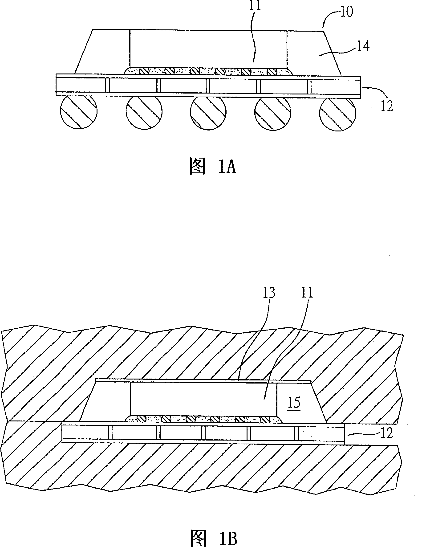
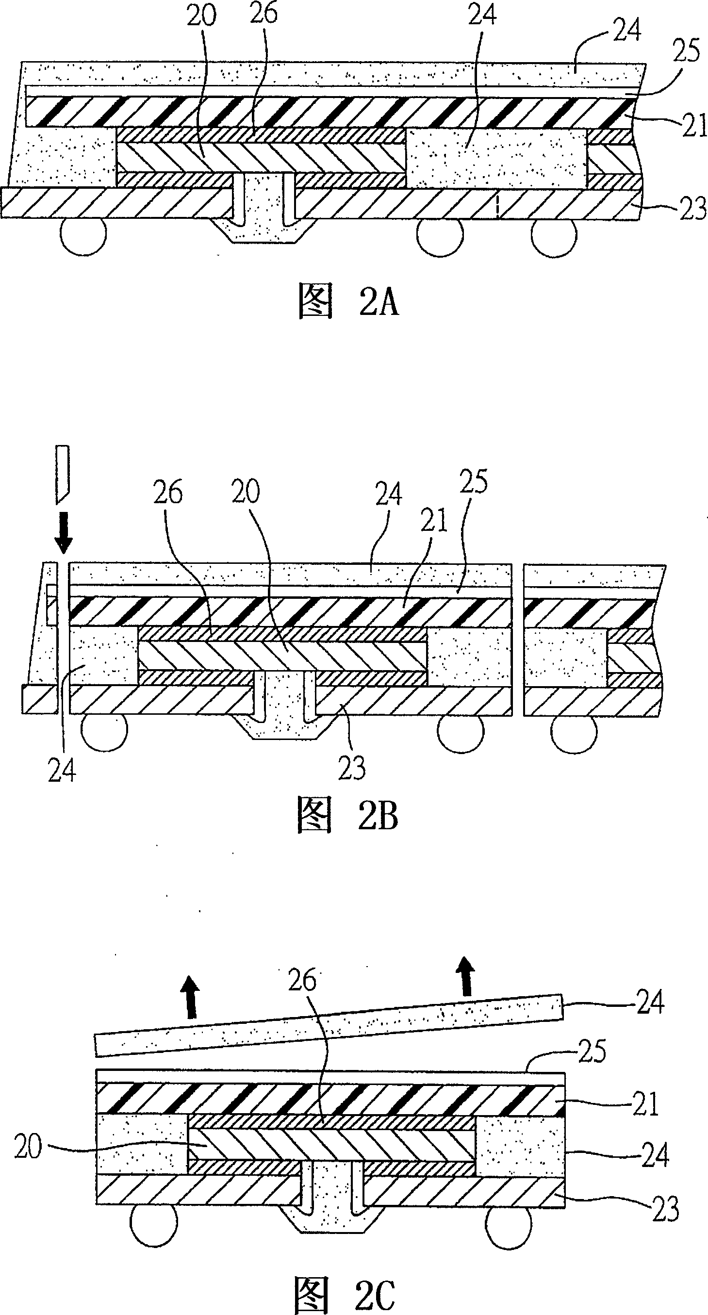
[0011] However, in the manufacturing process of the aforementioned semiconductor package, during the cutting step, because the cutting tool continues to cut through the heat sink, and because the heat sink is generally made of metal materials such as copper and aluminum, when cutting with a diamond knife,

Method used


Image

  • Heat-radiation type package structure and its method for making
  • Heat-radiation type package structure and its method for making
  • Heat-radiation type package structure and its method for making

Examples


no. 1 example

[0111] Referring to FIGS. 5A to 5F , they are schematic diagrams of the first embodiment of the heat dissipation package structure and its manufacturing method of the present invention.

[0112] As shown in FIG. 5A , firstly, the semiconductor chip 41 is placed and electrically connected to the chip carrier 42 , and an interface layer 43 is formed on the surface of the semiconductor chip 41 that is not placed on the chip carrier 42 .

[0113] The chip carrier 42 is, for example, a ball grid array (BGA) substrate or a land grid array (LGA) substrate, and the semiconductor chip 41 is, for example, a flip-chip semiconductor chip, and the flip-chip semiconductor chip passes through a plurality of The conductive bump 410 electrically connects its active surface to the chip carrier 42 .

[0114] The interface layer 43 can be, for example, a polyimide (Polyimide) film (P.I.tape) pasted on the semiconductor chip 41 as a substrate, or an epoxy resin (epoxy) coated on the semiconductor ...

no. 2 example

[0121] Referring to FIGS. 6A and 6B , they are schematic diagrams of a second embodiment of the heat dissipation package structure of the present invention. As shown in the figure, the heat-dissipating package structure of this embodiment is substantially the same as that of the preceding embodiments, the main difference being that after removing the interface layer and the encapsulant on the semiconductor chip 51, the encapsulant of the semiconductor chip 51 is also exposed. In the structure, an external heat sink (External Heat Slug) 56 is placed on the surface of the semiconductor chip 51 corresponding to the exposed encapsulant 54, and the external heat sink 56 can be generally planar (as shown in FIG. 6A ) or extended. A plurality of concave-convex structures (as shown in FIG. 6B ) are provided to provide good heat conduction effect of the semiconductor chip 51

no. 3 example

[0123] Referring to FIG. 7 , it is a schematic diagram of a third embodiment of the heat dissipation package structure of the present invention. As shown in the figure, the packaging structure of this embodiment is substantially the same as that of the preceding embodiments, the main difference being that a leaded semiconductor chip 61 is placed on a chip carrier 62, wherein the semiconductor chip 61 is separated from its passive surface. Connected to the chip carrier 62, and electrically connected to the chip carrier 62 through a plurality of bonding wires 67, and a material layer 68 such as a waste chip or a heat sink can be connected to the active surface of the semiconductor chip 61, And an interface layer (not shown) is provided on the material layer 68, so that after the chip carrier 62 is connected with the first heat sink 65 and the encapsulation and molding operation is completed, the cutting operation can be performed and the interface layer and the interface layer ca...


PUM


Abstract

The invention is concerned with the thermolysis packaging structure and the making method, it is: attaches the semiconductor chip with the chip carrying piece by electricity to form the surface or the second heat sink with surface, and attaches the first heat sink with thermolysis part that is opposites the open whole of the semiconductor chip and the support part, with the chip carrying piece, next, is forms the surface or the second heat sink with surface that covers the semiconductor chip and the packaging colloid of the first heat sink, and there is must certain space leaves for the packaging colloid covering the surface, which is the way of preventing the problems of pressure damage and glue overflow of the current making method, and to the next step is incises the packaging colloid follows the surface edge and removes the unwanted, losses heat for the semiconductor chip, in order to prevent the problems of raw edge and tools wastage, which reduces the cost efficiently.

Description

technical field [0001] The invention relates to a semiconductor packaging structure and a manufacturing method thereof, in particular to a heat-dissipating semiconductor packaging structure capable of effectively dissipating heat from a semiconductor chip and a manufacturing method thereof. Background technique [0002] With the demand for thinner, lighter and smaller electronic products, semiconductor packages integrating high-density electronic components and semiconductor chips of electronic circuits have gradually become the mainstream of packaging products. However, since the semiconductor package generates high heat during operation, if the heat of the semiconductor chip is not released immediately, the accumulated heat will seriously affect the electrical function and product stability of the semiconductor chip. On the other hand, in order to prevent the internal circuit of the package from being polluted by external water and dust, the surface of the semiconductor ch...

Claims


Application Information

Patent Timeline
IPC IPC(8): H01L21/50H01L23/36H01L23/31
CPCH01L24/97H01L2224/16225H01L2224/16245H01L2224/32225H01L2224/48091H01L2224/4824H01L2224/73204H01L2224/73215H01L2224/73265H01L2924/15311H01L2924/00014H01L2924/00
Inventor 黄建屏普翰屏蔡和易
Owner SILICONWARE PRECISION IND CO LTD
Why Eureka
Try Eureka