Method of producing group iii nitride substrate wafers and group iii nitride substrate wafers

A nitride and wafer technology, which is applied in semiconductor/solid-state device manufacturing, semiconductor/solid-state device parts, semiconductor devices, etc., can solve the problems such as no suggestion for III-nitride substrate wafer polishing technology

Inactive Publication Date: 2008-01-16
SUMITOMO ELECTRIC IND LTD
View PDF4 Cites 8 Cited by
  • Summary
  • Abstract
  • Description
  • Claims
  • Application Information

AI Technical Summary

Problems solved by technology

However, there are few recommendations for polis

Method used


Image

  • Method of producing group iii nitride substrate wafers and group iii nitride substrate wafers
  • Method of producing group iii nitride substrate wafers and group iii nitride substrate wafers
  • Method of producing group iii nitride substrate wafers and group iii nitride substrate wafers

Examples


Embodiment 1

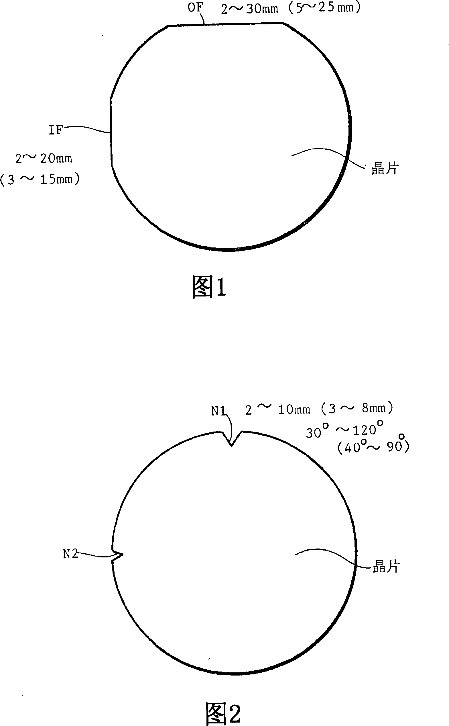
[0094] Aluminum oxide (Al 2 o 3 ) polishing plate of the disc. The ground, ground and polished sample wafers were 50 mm diameter and 0.5 mm thick GaN circular wafers in the HVPE grown state. The GaN ingot in the as-grown state is obtained by growing a GaN crystal on a GaAs lower substrate and removing the GaAs lower substrate. GaN substrate wafers in multiple growth states are fabricated by wire sawing GaN ingots. Each as-grown wafer had a 16 mm long orientation plane (OF). The central angle (Υ) of OF is 18 degrees. The removal width h of OF was 1.6 mm. Each sample is a set of wafers with three growth states of OF.

[0095] By heating the polished plate to a temperature of Tm + 30°C, rubbing the bottom of the polished plate with thermoplastic solid wax to soften the wax, placing the wafer in the grown state at a margin p (p = 5 mm) of 5 mm from the edge of the plate and removing the grown state The wafer was pressed to the polishing plate to stick three as-grown GaN waf...

Embodiment 2

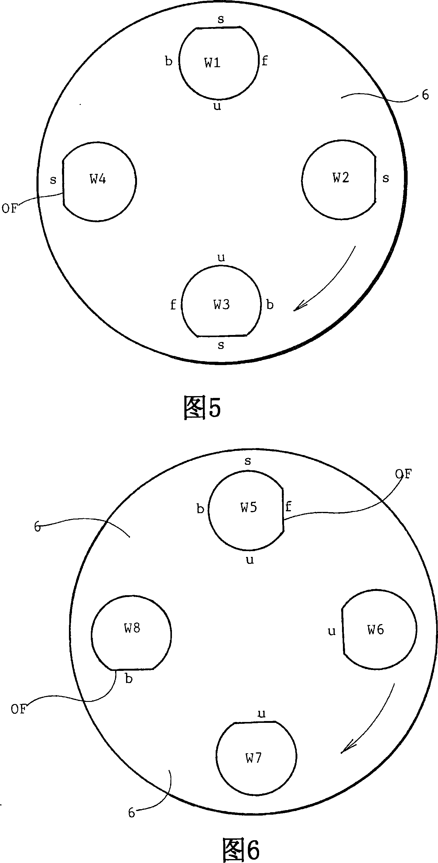
[0123] Embodiment 2 adopts aluminum oxide (Al 2 o 3 ) polishing plate of the disc. The target GaN wafer for the grinding, lapping and polishing processes is a GaN wafer in the HVPE growth state with a multi-group band structure with a diameter of 50 mm and a thickness of 0.5 mm. The banded structure refers to a heterogeneous GaN crystal with alternating groups of parallel low-density single-crystal regions and parallel defect-accumulated regions. It has been prepared by preparing a GaAs lower substrate, fabricating a tape mask on the GaAs lower substrate, growing a GaN film crystal on the tape masked lower substrate by the HVPE method, making a polished surface, and maintaining the polished surface until the end , GaN wafers with ribbon structure were prepared. GaN / GaAs synthesis wafers in the HVPE growth state were prepared. As-grown GaN free-standing wafers were obtained by removing the GaAs underlying substrate and beveling the edges. Alternatively, if a tall GaN cryst...


PUM

PropertyMeasurementUnit
Diameteraaaaaaaaaa
Thicknessaaaaaaaaaa
Diameteraaaaaaaaaa

Abstract

Quality of one-surface planar processed group 3 nitride wafers depends upon a direction of pasting of wafers on a polishing plate. Low surface roughness and high yield are obtained by pasting a plurality of group 3 nitride as-grown wafers on a polishing plate with OFs or notches facing forward (f), backward (b) or inward (u) with thermoplastic wax having a thickness of 10[mu]m or less, grinding the as-grown wafers, lapping the ground wafers, polishing the lapped wafers into mirror wafers with a bevel of a horizontal width of 200[mu]m or less and a vertical depth of 100[mu]m or less.

Description

[0001] related application [0002] This application claims the priority of Japanese Patent Application No. 2006-191000 filed on July 12, 2006 and Japanese Patent Application No. 2006-337678 filed on December 15, 2006. technical field [0003] The invention relates to pasting a grown GaN, AlN or AlGaN substrate wafer to a polishing plate and grinding, fine grinding and polishing the grown wafer into a mirror wafer. GaN, AlN and AlGaN wafers are now collectively referred to as "III-nitride" wafers. All III-nitride crystals cannot grow from the liquid phase. As-grown substrate crystals of Ill-nitrides are fabricated by growing a thick film on the lower substrate in the vapor phase, removing the lower substrate and obtaining a self-supporting wafer. [0004] Silicon (Si) substrate wafers are flexible. For silicon wafers, it is easy to grind, fine grind and polish. GaN is stiffer than silicon, but more brittle than silicon. GaN can withstand much more external shock than Si. ...

Claims


Application Information

Patent Timeline
IPC IPC(8): H01L21/304H01L23/00B24B1/00
Inventor 石桥惠二入仓正登中畑成二
Owner SUMITOMO ELECTRIC IND LTD
Why Eureka
Try Eureka