Phase change memory with diode unit selective connection and its making method

A phase-change storage and diode technology, which is applied in the field of microelectronics, can solve the problems of inability to realize multi-layer stacking of energy storage units, complex formation process of diode gating tube units, etc., and achieve the effect of increasing storage density

Inactive Publication Date: 2008-01-16
FUDAN UNIV +1
View PDF1 Cites 18 Cited by
  • Summary
  • Abstract
  • Description
  • Claims
  • Application Information

AI Technical Summary

Problems solved by technology

Therefore, the currently reported phase-change memory cells can only be formed on a single crystal silicon substrate, which has the disadvantages of complex formation process of the diode gating tube unit, and the inability to realize multi-layer stacking of memory cells, thus restricting the further improvement of its storage density.

Method used


Image

  • Phase change memory with diode unit selective connection and its making method
  • Phase change memory with diode unit selective connection and its making method
  • Phase change memory with diode unit selective connection and its making method

Examples


Embodiment approach 1

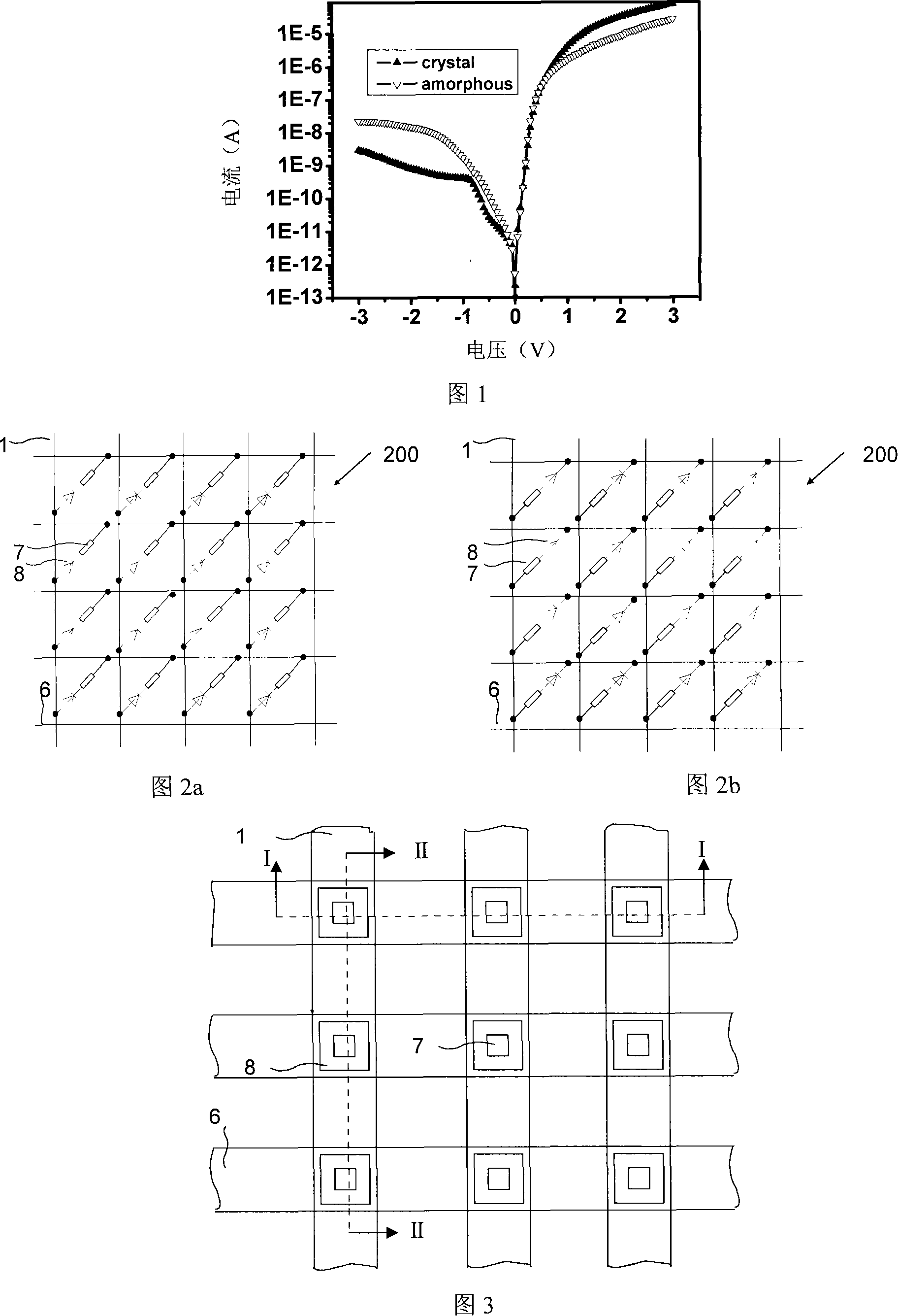
[0060] 2a and 2b are schematic diagrams of array cells based on a phase-change memory using diode gating, and the array is denoted by reference numeral 200 . As shown in FIG. 2 , it includes four bit lines 1 and four word lines 6 , and the word lines 6 and bit lines 1 are connected by phase change material resistance units 8 and diode units 7 . In FIG. 2a, the word line 6 is directly connected to the phase change material unit 8, and the bit line 1 is directly connected to the diode unit 7; in FIG. 2b, the bit line 6 is directly connected to the phase change material unit 8, and the word line 1 is directly connected to the diode unit 7. The peripheral reading and writing circuit modules of the storage array are omitted here.

[0061] FIG. 3 is a plan view of the array 200 shown in FIG. 1 . The phase-change material unit 8 and the diode unit 7 are formed at the intersection of the word line 6 and the bit line 1 . The sizes of the phase-change material unit 8 and the diode unit...

Embodiment approach 2

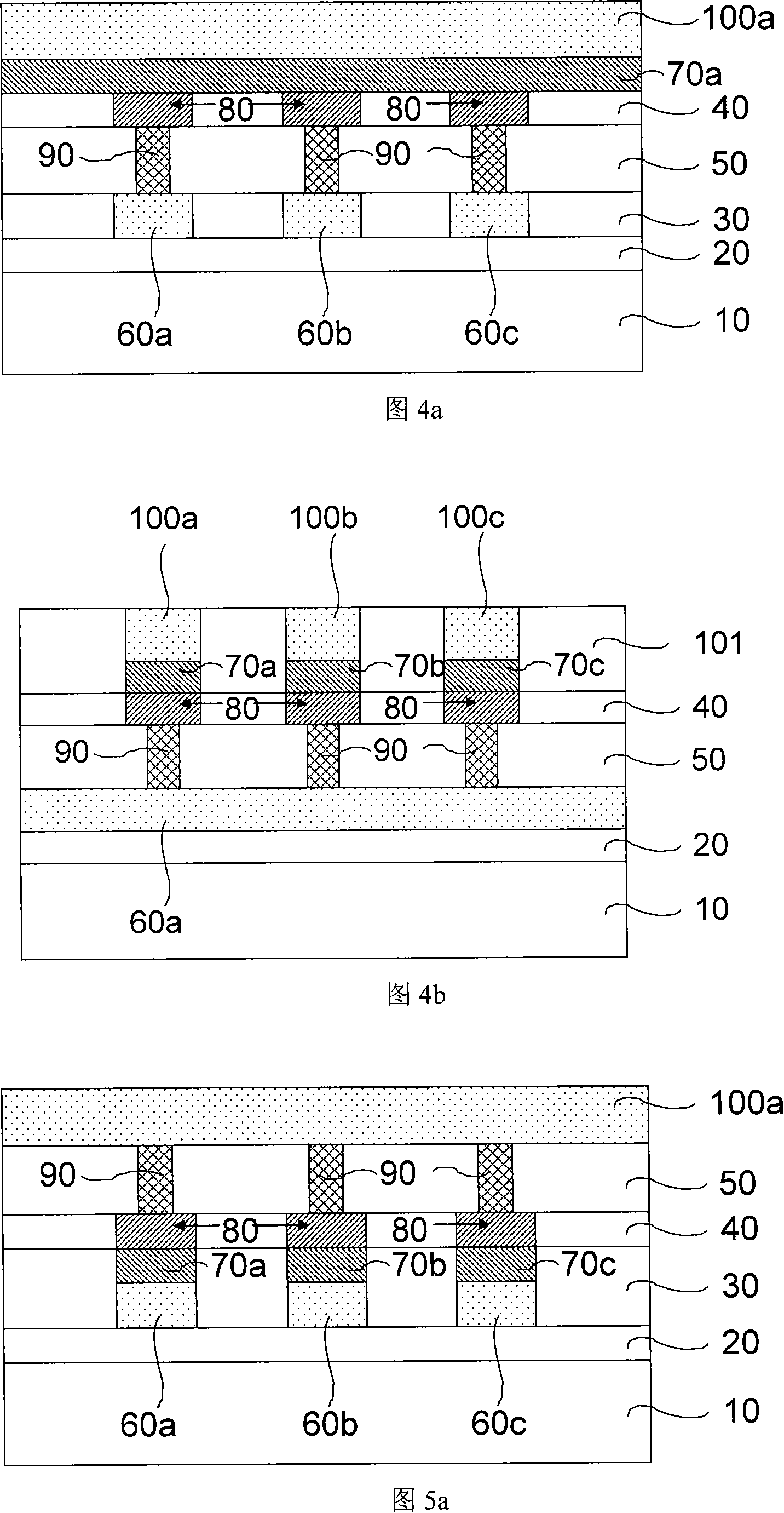
[0082] The following is a phase-change memory based on a Schottky diode formed by a metal electrode and a manufacturing method thereof. Two different examples are specifically disclosed, the main difference being whether the gate diode is formed between the word line and the phase change film material or between the bit line and the phase change film material.

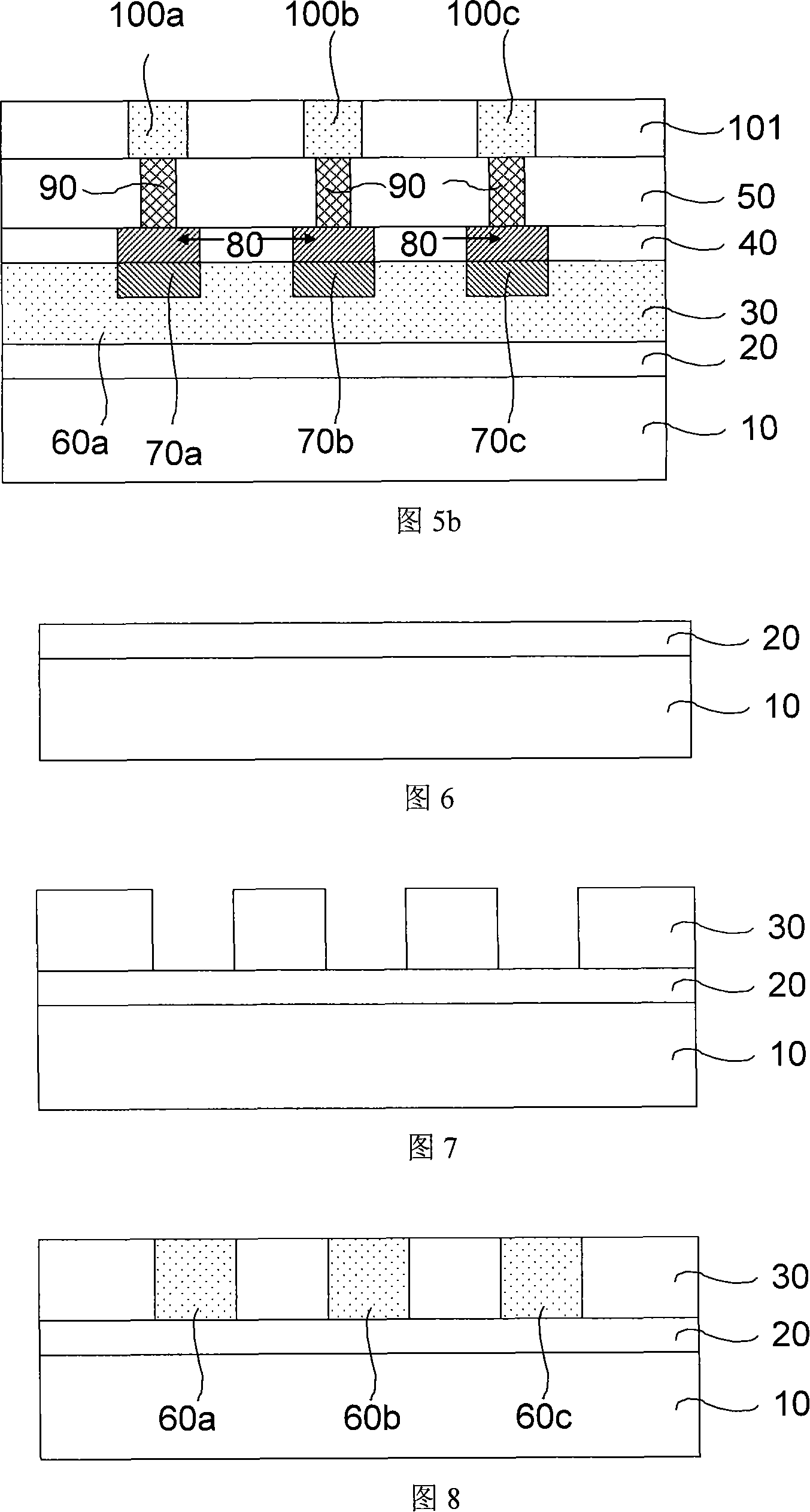
[0083] Figures 14a and 14b are schematic diagrams of the memory structure of different cross-sections of one example (the diode shown in Figure 2b is directly connected to the word line), and Figure 14a and Figure 14b are another example (the diode shown in Figure 2a is directly connected to the bit line). Schematic diagram of the cross-sectional memory structure. Figures 14a and 15a are I-I cross-sectional views of Figure 3 in the embodiment of the present disclosure, and Figures 14b and 15b are II-II cross-sectional views of Figure 3 in the embodiment of the present disclosure.

[0084] One of the examples is shown ...


PUM


Abstract

The invention pertains to the field of microelectronic technology, specifically to a phase-change memory based on diode unit gating and the fabrication method thereof. The phase-change memory comprises word lines with the properties of semiconductor thin film, one or more metal electrodes, phase-change materials with the properties of semiconductor thin film, and site lines with the properties of semiconductor thin film. Heterojunction diodes formed by the word lines or the site lines and the phase-change thin-film materials, or Schottky diodes formed by the word lines or the site lines and the metal electrodes serve as gating units of the memory in a structure of 1D/1R. The phase-change memory in the invention is simple in structure management and fabrication method, and independent of the silicon substrate. The array stacking of a plurality of phase-change memories can be realized, and thereby the memory density is greatly increased.

Description

technical field [0001] The invention belongs to the technical field of microelectronics, and in particular relates to a phase-change memory device and a manufacturing method thereof, in particular to a phase-change memory based on diode unit gating and a manufacturing method thereof. Background technique [0002] As an emerging non-volatile storage technology, phase change memory has great advantages over FLASH in many aspects such as read and write speed, read and write times, data retention time, unit area, and multi-value realization, and has become the current non-volatile storage technology. The focus of technology research. The continuous progress of phase change memory technology makes it one of the most powerful competitors for mainstream products in the future non-volatile memory technology market [1] . [0003] The phase change memory uses chalcogenide materials, such as Ge-Se-Te (hereinafter referred to as GST), which can realize the conversion between amorphous...

Claims


Application Information

Patent Timeline
Patent Type & Authority Applications(China)
IPC IPC(8): H01L27/24H01L23/528H01L21/84H01L21/768G11C11/56
Inventor 林殷茵唐立汤庭鳌陈邦明
Owner FUDAN UNIV
Why Eureka
Try Eureka