Waveform shaping circuit

A waveform shaping and circuit technology, which is applied in multiple input and output pulse circuits, non-electrical signal transmission systems, signal transmission systems, etc., can solve the problem of large dynamic range of infrared data receiving circuits, signals that cannot be restored by shaping, and photocurrent drop To avoid problems such as slowing down, achieve good dynamic performance, simple structure, and increase the effective distance

Inactive Publication Date: 2008-02-06
史宝祥
View PDF1 Cites 8 Cited by
  • Summary
  • Abstract
  • Description
  • Claims
  • Application Information

AI Technical Summary

Problems solved by technology

The remote control distance of the general infrared remote control system is 3-5 meters, and the remote control effect is quite poor when it exceeds 5 meters. When the remote control battery power is weak and other interference factors are large, the effective distance of the remote control is less than 3 meters, or even Shorter
[0012] There are two problems in this circuit. One is that at different distances, the output current of the infrared photodiode varies greatly due to the different light intensity, generally from hundreds (nA) to t

Method used


Image

  • Waveform shaping circuit
  • Waveform shaping circuit
  • Waveform shaping circuit

Examples


Embodiment Construction

[0046] The present invention will be further described below in conjunction with the accompanying drawings and specific embodiments.

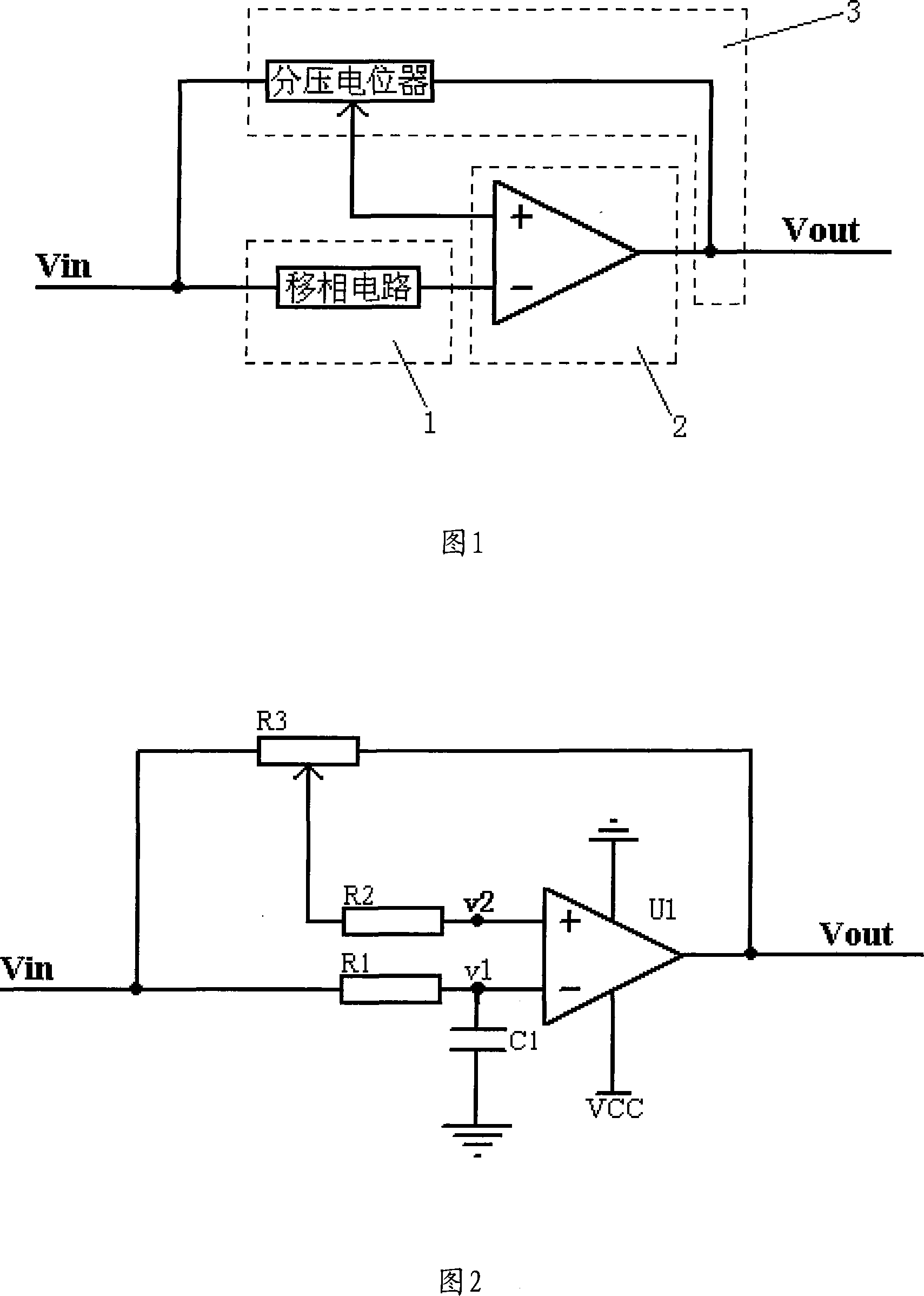
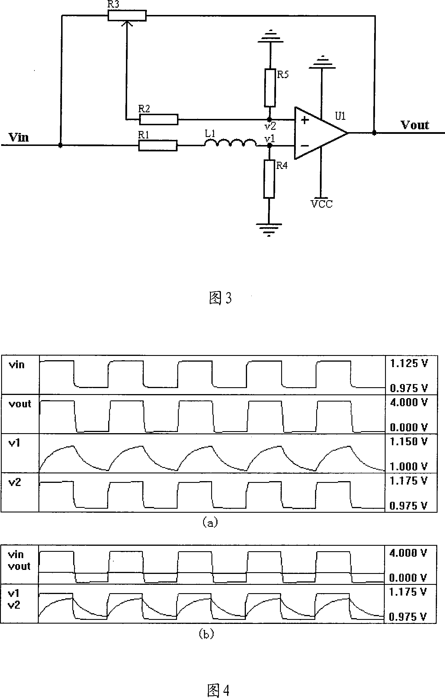
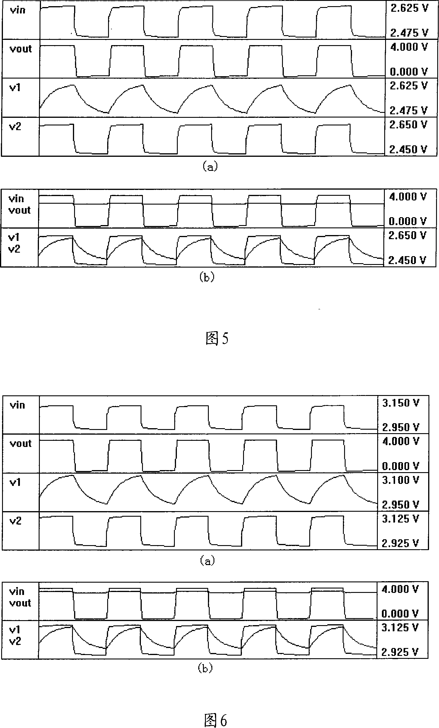
[0047] Referring to Fig. 2 and Fig. 3 are two examples of the present invention, in the figure R1. Impedance matching resistance, R2. Impedance matching resistance, R3. Feedback voltage divider adjustment resistance, R4. Impedance matching resistance, R5. Impedance matching resistance, U1. Integrated amplifier circuit, C1. Phase-shifting capacitor, L1. Phase-shifting inductor, Vin. Waveform input terminal, Vout. Waveform output terminal.

[0048] The input signal Vin is respectively connected to two input terminals of the comparator through a phase shift circuit and a feedback circuit.

[0049] The phase shifting circuit is as follows: the input signal Vin passes through the impedance matching resistor R1, and then one end of the hysteresis capacitor C1 is connected to the inverting input end of the comparator, and the other end of the hysteres...


PUM


Abstract

The present invention relates to a circuit which can reshape waveform of any base value voltage and peak value voltage into regular square wave. The prior waveform reshaping circuit produces a threshold value for comparing through a complex threshold value calculating circuit; and then reshapes the waveform, thereby having the shortcomings of complex structure and poor reshaping efficiency. The present invention reshapes the waveform through a method of delaying comparison. The reshaping circuit is a capacitance or inductance which backward moves the phase of the input waveform and a positive feedback circuit which consists of a voltage dividing resistor used for adjusting the noise margin, so that the waveform of any base value and peak value is reshaped into regular square wave to beneficial for the digital disposal. Thereby the present invention has a good reshaping efficiency. When in use of the infrared data communication system, the present invention has the advantages of greatly increasing the transmission speed and the transmission distance, well overcoming the various unbeneficial factors such as ambient light, photodiode current leakage and transmission power, and not being influenced by the trialing problem which is produced by the PIN when in high speed infrared communication.

Description

technical field [0001] The invention relates to a waveform shaping circuit, in particular to a circuit capable of shaping arbitrary base voltage and peak voltage waveforms into regular square waves. technical background [0002] In the waveform shaping circuit, the base value of many waveforms, especially the waveform at the infrared receiving end, is generally an unknown voltage level, and affected by ambient light and other factors, the voltage value varies in a large range, which is not conducive to waveform shaping; Due to the above factors, it is not conducive to the shaping of the waveform. [0003] At present, the existing waveform shaping systems at the infrared receiving end can be divided into two categories according to the complexity. One is the basic waveform shaping system, as shown in Figure 7. This type of circuit has a simple structure and is widely used, and is mostly used for infrared remote control. In order to enhance the receiving ability of this type...

Claims


Application Information

Patent Timeline
IPC IPC(8): H03K5/24G08C23/04
Inventor 史宝祥
Owner 史宝祥
Why Eureka
Try Eureka