Forming method for contact hole

A contact hole and sidewall layer technology, applied in electrical components, semiconductor/solid-state device manufacturing, circuits, etc., can solve problems such as device performance drift, avoid over-etching, enhance protection, and prevent channel damage.

Active Publication Date: 2008-02-13
SEMICON MFG INT (SHANGHAI) CORP
View PDF1 Cites 8 Cited by
  • Summary
  • Abstract
  • Description
  • Claims
  • Application Information

AI Technical Summary

Problems solved by technology

However, this method cannot solve the problem that the sidewall layer of the gate is easily completely removed after the etch stop layer is removed by etching, resulting in a drift in device performance.

Method used


Image

  • Forming method for contact hole
  • Forming method for contact hole
  • Forming method for contact hole

Examples


Embodiment Construction

[0026] In order to make the above objects, features and advantages of the present invention more comprehensible, specific implementations of the present invention will be described in detail below in conjunction with the accompanying drawings.

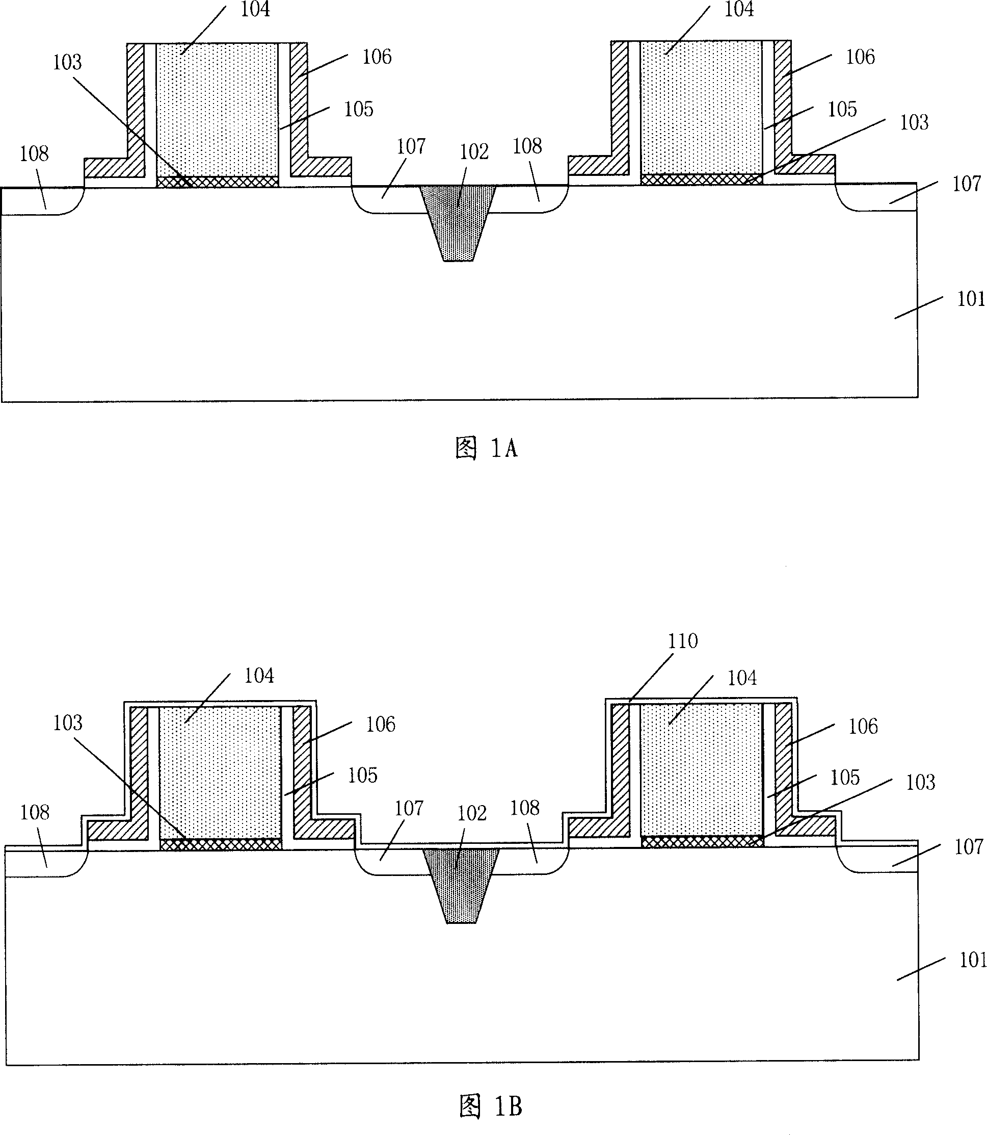
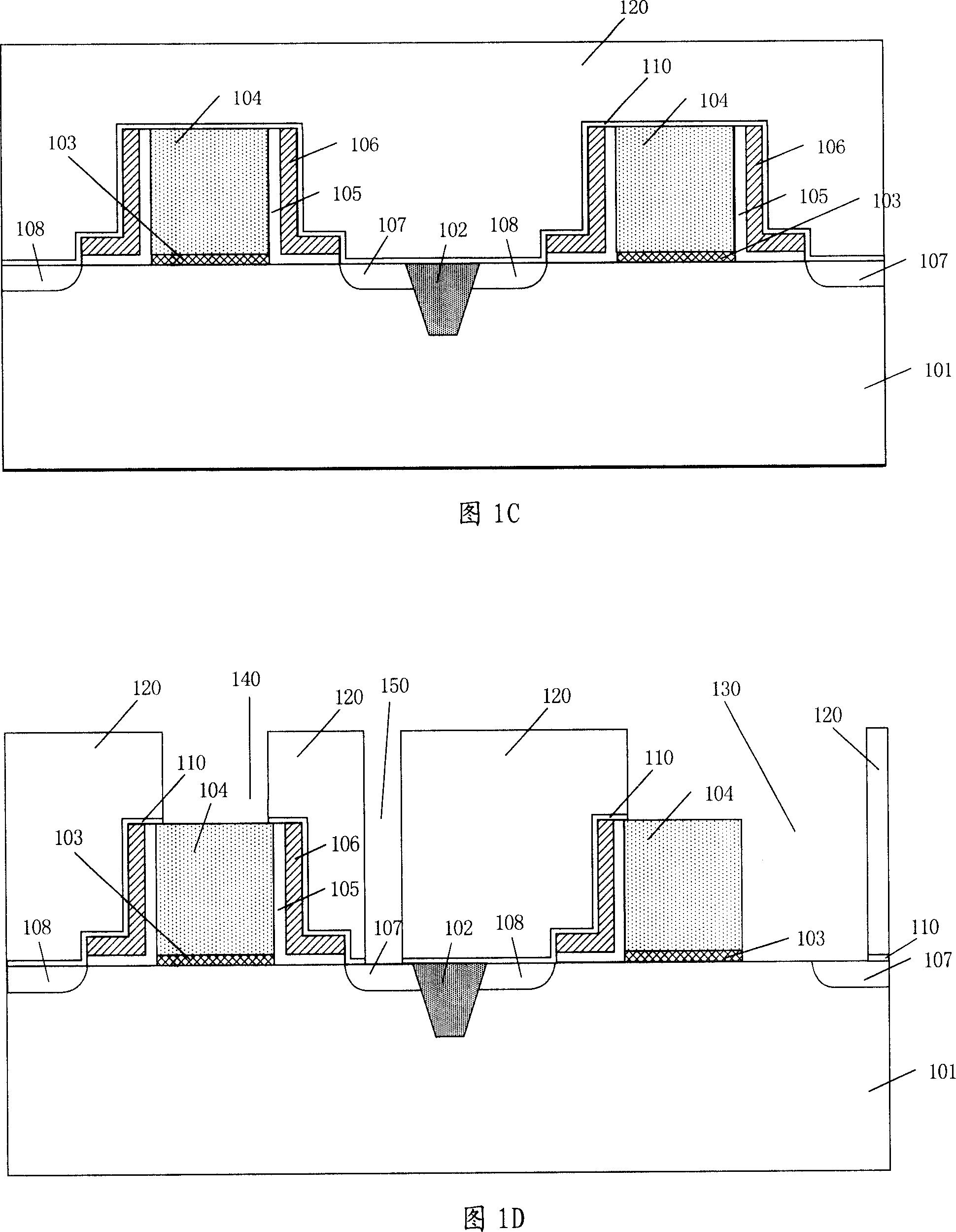
[0027] In the method for forming the contact hole of the present invention, before forming the etching stop layer, an additional dielectric layer is deposited, and after anisotropic etching, it remains only on the gate sidewall to form an additional sidewall layer, It is equivalent to thickening the thickness of the gate sidewall layer, which enhances the protection degree of the gate sidewall during the etching process of the interlayer dielectric layer, and avoids the exposure of the gate sidewall after etching to cause damage to the device channel and performance. drift.

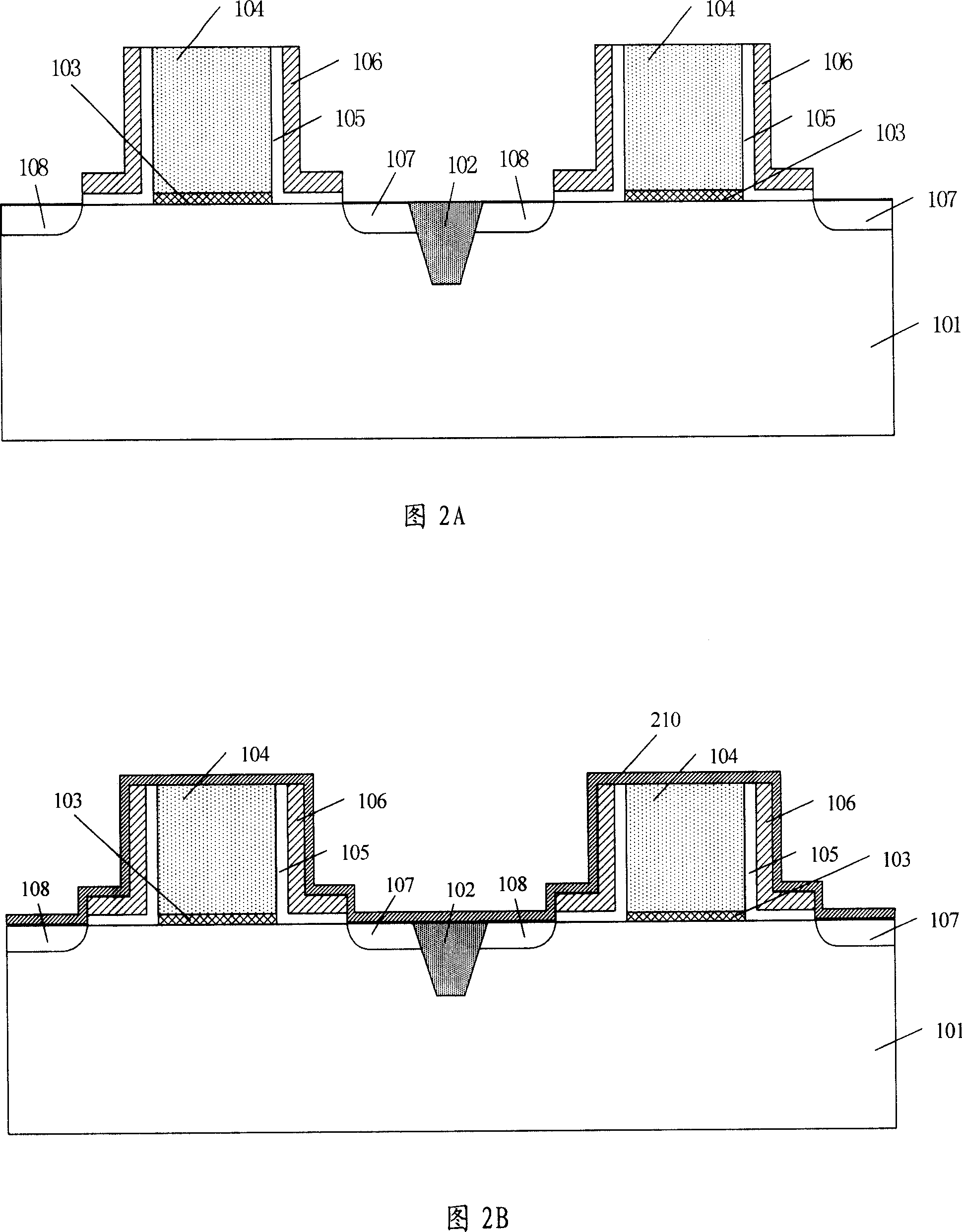
[0028] 2A to 2F are schematic views of the contact hole forming method of the present invention. FIG. 3 is a process flow chart of the contact hole forming metho...


PUM


Abstract

A method for forming contact holes is disclosed and comprises: an underlayer, on which a plurality of grids is formed, is provided and the side walls of the grids have side wall layers; an added medium layer is deposited on the undeerlayer; the added medium layer is corroded and added side wall layers are formed at the side walls of the grids; a corroding and stopping layer is deposited on the underlayer; an interlaminar medium layer is deposited on the corroding and stopping layer; the interlaminar medium layer is made into a design and is corroded to form contact holes. The invention, through thickening the thickness of the side wall layer of the grids, strengthens the protection of the side wall of the grids, avoids over-corrosion of side wall layers, prevents the damage of groove and the drift of the device properties, and increases the rate of finished products and the reliability of devices while the device parameter remains the same.

Description

technical field [0001] The invention relates to the technical field of semiconductor manufacturing, in particular to a method for forming a contact hole. Background technique [0002] The manufacture of semiconductor integrated circuits is an extremely complex process, the purpose of which is to reduce the various electronic components and circuits required for a specific circuit on a small-area wafer. Wherein, each component must be electrically connected by an appropriate interconnecting wire, so as to exert the desired function. [0003] As the production of integrated circuits develops toward ultra-large-scale integrated circuits (ULSI), the internal circuit density is increasing. As the number of components contained in the chip continues to increase, the available space for surface wiring is actually reduced. The solution to this problem is to adopt a multi-layer metal wire design, and use a multi-layer connection in which a multi-layer insulating layer and a conducti...

Claims


Application Information

Patent Timeline
Patent Type & Authority Applications(China)
IPC IPC(8): H01L21/768H01L21/311
Inventor 宋伟基朱旋陈昱升毛刚
Owner SEMICON MFG INT (SHANGHAI) CORP
Why Eureka
Try Eureka