Integrated circuit packaging construction and multi-layer conducting wire holder used for it

A technology of integrated circuit and lead frame, which is applied in the field of integrated circuit packaging structure, to achieve the effect of increasing the application range of chip packaging and increasing position selectivity

Inactive Publication Date: 2008-02-27
CHIPMOS TECH INC
View PDF0 Cites 10 Cited by
  • Summary
  • Abstract
  • Description
  • Claims
  • Application Information

AI Technical Summary

Problems solved by technology

[0007] The main purpose of the present invention is to overcome the defects of the existing integrated circuit packaging structure, and provide a new integrated circuit packaging structure and the multilayer lead frame used therein. The technical problem to be solved is to make it through the multilayer The lead frame and the electrical transfer element at least partially outside the bonding hot zone can solve the electrical short circuit caused by the overly dense interlacing of bonding wires in the bonding hot zone, thereby increasing the application range of the chip package with the lead frame as the chip carrier , which is more suitable for practical

Method used


Image

  • Integrated circuit packaging construction and multi-layer conducting wire holder used for it
  • Integrated circuit packaging construction and multi-layer conducting wire holder used for it
  • Integrated circuit packaging construction and multi-layer conducting wire holder used for it

Examples


no. 1 Embodiment

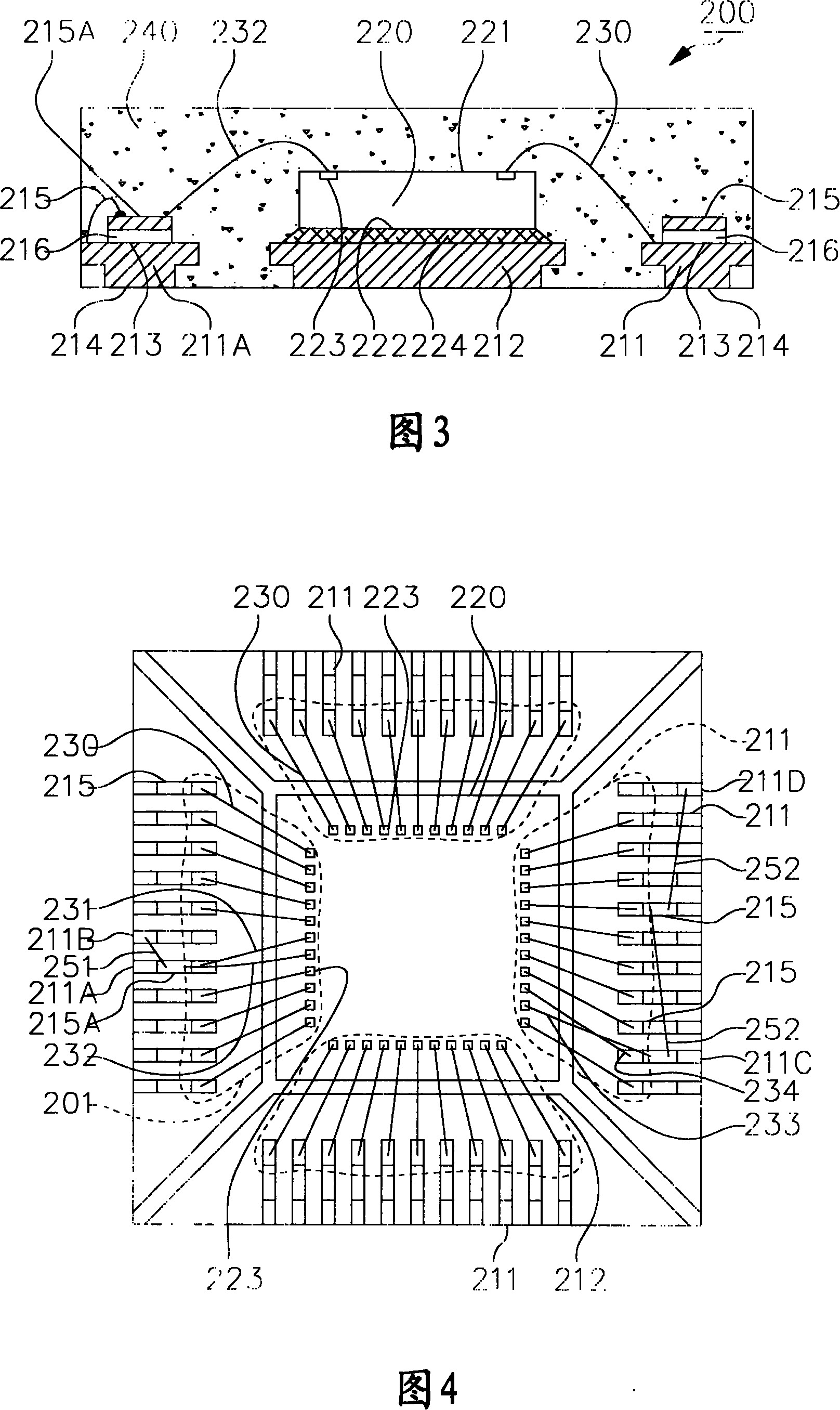
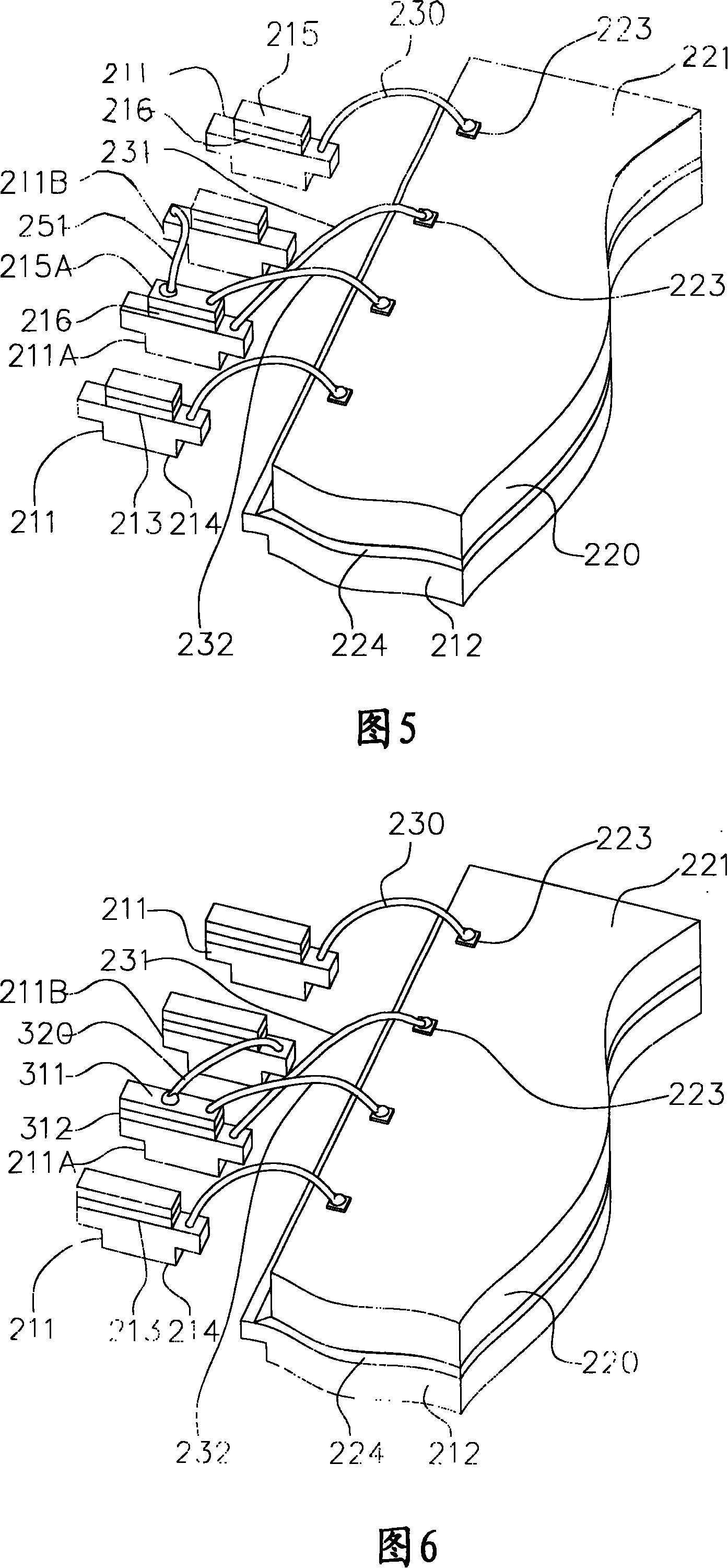
[0066] Please refer to FIG. 3, FIG. 4 and FIG. 5. FIG. 3 is a schematic cross-sectional view of an integrated circuit packaging structure according to a first preferred embodiment of the present invention, and FIG. 4 is a front perspective schematic view of the integrated circuit packaging structure. Fig. 5 is a partial perspective view. According to a first embodiment of the present invention, an integrated circuit packaging structure is disclosed. The integrated circuit package structure 200 mainly includes a multi-layer lead frame, a chip 220 , a plurality of bonding wires 230 and at least one electrical transfer element 251 , 252 .

[0067] The multi-layer lead frame has a plurality of pins 211 and at least one transition finger 215 (or can be called a transition island), each pin 211 has an upper surface 213 and a lower surface 214, and the transition fingers 215 are mounted on the upper surface 213 of one of the pins 211 . In this embodiment, based on the convenience a...


PUM


Abstract

The present invention relates to an IC packaging and its multi-layer conductor frame. The IC packaging has been defined with a wire-bonded region which mainly includes a multi-layer conductor frame with pins, a wafer, even numbers of welding lines in this region and at least an electric-transferred component. At least one of these pins carries a transferred finger which is insulating to the corresponding pin and does not cover inner terminal of the pin. The electric-transferred component has at least one part which is formed outside the wire-bonded region, and the transferred finger is connected to one pin which is not under the transferred finger. The shortest distance between staggered welding lines can be added, or staggered points of these welding lines can be reduced, thus staggered short circuit of welding lines can be avoided during colloid sealing.

Description

technical field [0001] The present invention relates to an integrated circuit packaging structure, in particular to a kind of electric switching element that can solve the electrical short circuit caused by the over-dense welding wire interlacing in the bonding hot zone, and further increase the number of chips that use the lead frame as the chip carrier. The scope of application of the package, and the use of the electrically independent transfer finger coverage area on the lead frame can increase the position of the electrical transfer element connected to the lead frame pin. Selectively use the integrated circuit package structure of the multi-layer lead frame and its use multi-layer lead frame. Background technique [0002] In known packaging technologies, the chip carrier can be a leadframe or a wiring substrate. The lead frame has the advantage of low cost and easy acquisition, but the pins cannot be cross-arranged, so it is not suitable for packaging chips with compl...

Claims


Application Information

Patent Timeline
Patent Type & Authority Applications(China)
IPC IPC(8): H01L23/488H01L23/495H01L23/50
CPCH01L2224/32245H01L2924/19107H01L2224/73265H01L2224/48247H01L2224/48465H01L2224/4911H01L2924/181H01L2224/05554H01L2924/00H01L2924/00012
Inventor 毛苡馨陈雅琪林峻莹陈煜仁
Owner CHIPMOS TECH INC
Why Eureka
Try Eureka