
Method, tool, and apparatus for manufacturing a semiconductor device

一种半导体、工具的技术,应用在制造半导体器件领域,能够解决去除沉积膜、半导体基板或生产线污染、难加热半导体基板等问题,达到防止金属污染、接触面积增加的效果

Inactive Publication Date: 2008-03-05
SHINDENGEN ELECTRIC MFG CO LTD +1
View PDF1 Cites 3 Cited by
  • Summary
  • Abstract
  • Description
  • Claims
  • Application Information

AI Technical Summary

Problems solved by technology

[0015] As described above, the conventional technology has a problem that it is difficult to heat a semiconductor substrate in a vacuum
In addition, the method disclosed in Patent Document 1 has the problem that it is difficult to remove the deposited film after heat treatment, and there is also the problem that the semiconductor substrate or the production line is contaminated with metal

Method used


Image

  • Method, tool, and apparatus for manufacturing a semiconductor device
  • Method, tool, and apparatus for manufacturing a semiconductor device
  • Method, tool, and apparatus for manufacturing a semiconductor device

Examples


Embodiment Construction

[0082] Hereinafter, embodiments according to the present invention will be described with reference to the drawings.

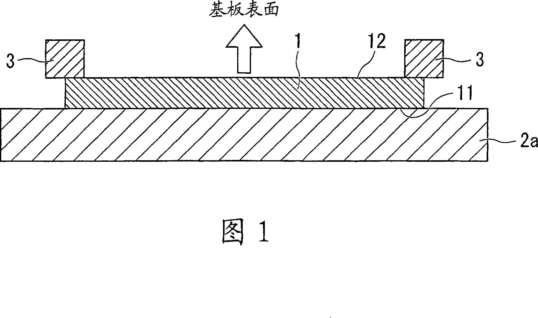
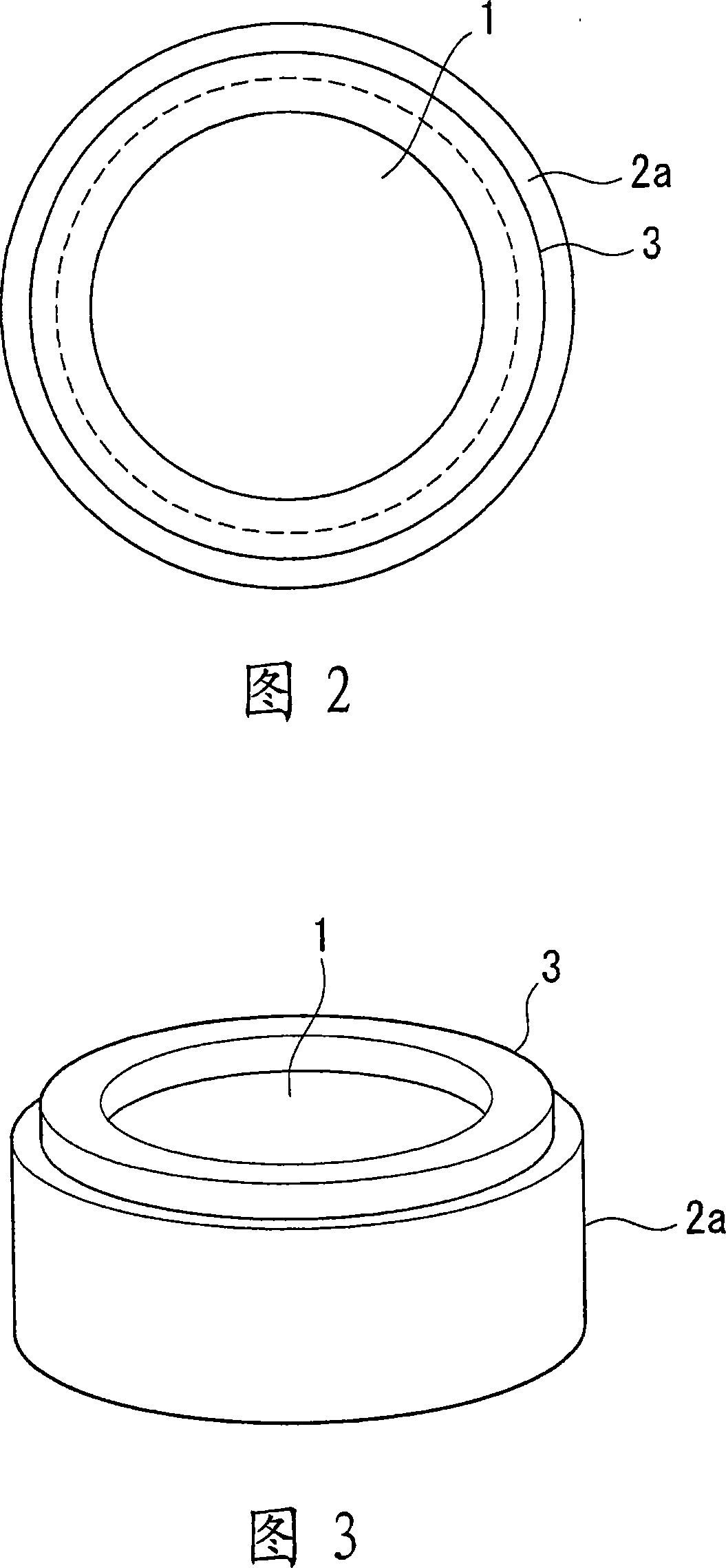
[0083] Hereinafter, a first embodiment will be described in which the semiconductor substrate is heated in the state shown in FIGS. 1 to 3.

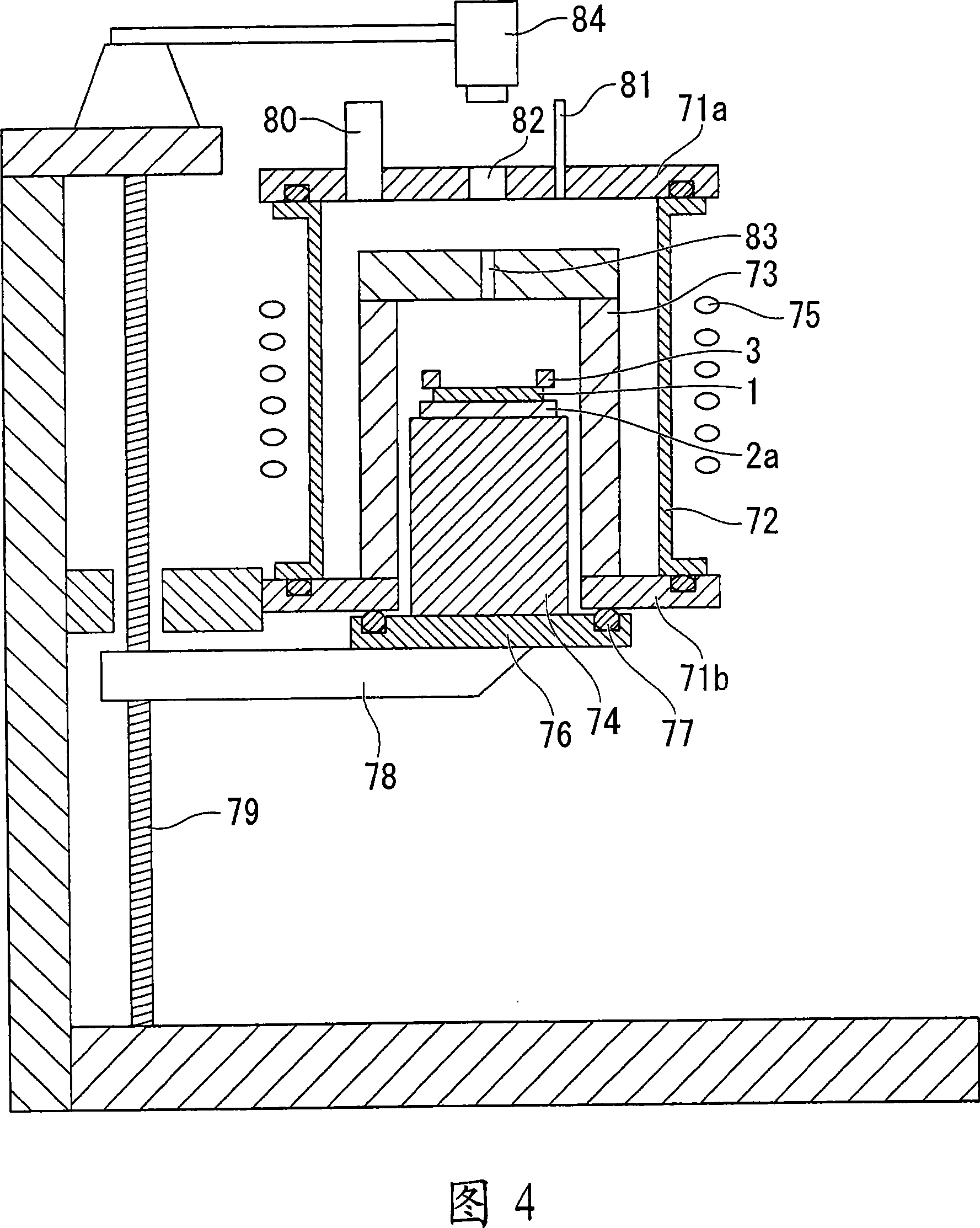
[0084] FIG. 1 is a cross-sectional view showing a tool and a WBG substrate (as a semiconductor substrate) in the first embodiment. Fig. 2 is a plan view showing a tool and a WBG substrate in the first embodiment. Fig. 3 is a perspective view showing a tool and a WBG substrate in the first embodiment.

[0085] The WBG substrate 1 is placed on the susceptor 2a (the main component of which may be graphite (C)) in such a way that the main surface 11 of the WBG substrate 1 faces the susceptor 2a. A heavy stone 3 is placed on the other main surface 12 of the WBG substrate 1. According to the present invention, the above-mentioned base 2a and heavy stone 3 serve as tools for manufacturing semiconductor devices.

[0086] Due to the ...


PUM


Abstract

A method of manufacturing a semiconductor device, includes increasing adherence between a susceptor as a heating element, and a semiconductor substrate disposed on the susceptor, by using an adherence increasing mechanism, or increasing heat transmitted to a semiconductor substrate, which is disposed on a susceptor as a heating element, by using a transmitted-heat increasing mechanism; and heating the semiconductor substrate to have a predetermined temperature by heating the susceptor. The adherence increasing mechanism may include the susceptor and one of a heavy-weight stone disposed on the semiconductor substrate, a cap disposed on the semiconductor substrate and engaged with the susceptor, and an adhesive layer provided between the susceptor and the semiconductor substrate. The transmitted-heat increasing mechanism may include the susceptor and small pieces which are disposed on the semiconductor substrate and have radiated-light absorption ability. The susceptor may hold a plurality of the semiconductor substrates in a stacked form.

Description

Technical field [0001] The present invention relates to a method of manufacturing a semiconductor device, which method includes a step of heating a semiconductor substrate in a vacuum. The present invention also relates to a tool for manufacturing a semiconductor device used in the above steps, and a related apparatus for manufacturing a semiconductor device. Background technique [0002] Compared with silicon (Si), wide band gap (WBG) semiconductors such as silicon carbide (SiC) or gallium nitride (GaN) have a wider band gap, and therefore are materials with excellent voltage resistance and heat resistance characteristics. Therefore, they are expected to become potential materials for power devices. The structure of WBG power devices currently being actively researched and developed is mainly divided into Schottky barrier diodes (SBD), PiN junction diodes (PiND), MOS (metal oxide semiconductor) transistors, and junction transistors. The structure of the SBD and junction transist...

Claims


Application Information

Patent Timeline
Patent Type & Authority Applications(China)
IPC IPC(8): H01L21/683H01L21/324
CPCH01L21/68721H01L29/6606H01L29/1608H01L21/67103H01L21/67115Y10T29/49117Y10T29/49124H01L21/324H01L21/477
Inventor 西川恒一清水正章野中贤一横山诚一桥本英喜
Owner SHINDENGEN ELECTRIC MFG CO LTD
Learn More