

Optical amplifier gain noise compensation method and apparatus
A noise compensation, optical amplifier technology, applied in electromagnetic wave transmission systems, electrical components, transmission systems, etc., to achieve the effect of convenient engineering application and great application value
- Summary
- Abstract
- Description
- Claims
- Application Information
AI Technical Summary
Problems solved by technology
Method used
Image

Examples
no. 1 example
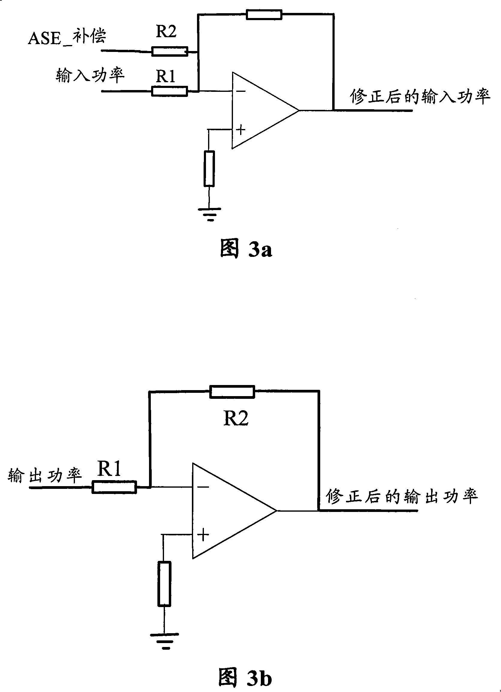
[0051] Fig. 3a is a view of a noise compensation circuit implemented based on an operational amplifier according to the first embodiment of the present invention.
[0052] Referring to Fig. 3a, in this embodiment, the gain control is realized by a hardware analog closed-loop circuit, and the noise power compensation circuit is realized by an operational amplifier, and the main method is to pressurize (add current) at the input end of the EDFA, that is, realize by an adder.
[0053] As shown in Figure 3a, since the ASE power is a fixed value for a fixed gain, that is to say, the PASE is a fixed power, and the incident light detection of the EDFA is a linear detection, so it is only necessary to add A fixed voltage value, as the equivalent incident light detection voltage, can realize the compensation function of ASE noise. Therefore, the corrected incoming light and the corresponding outgoing light signal are the final equivalent control parameters for gain locking control.
no. 2 example
[0055] Fig. 3b is a view of a noise compensation circuit implemented based on an operational amplifier according to a second embodiment of the present invention.
[0056] Referring to FIG. 3b, the gain control is also implemented by a hardware analog closed-loop circuit, and the noise power compensation circuit is implemented by an operational amplifier, that is, by a subtractor. The main method is to divide the voltage (shunt) at the output end of the EDFA. Different from Fig. 3a, in this embodiment, a fixed voltage value is added to the end of the light detection branch, so as to realize the compensation function of ASE noise.
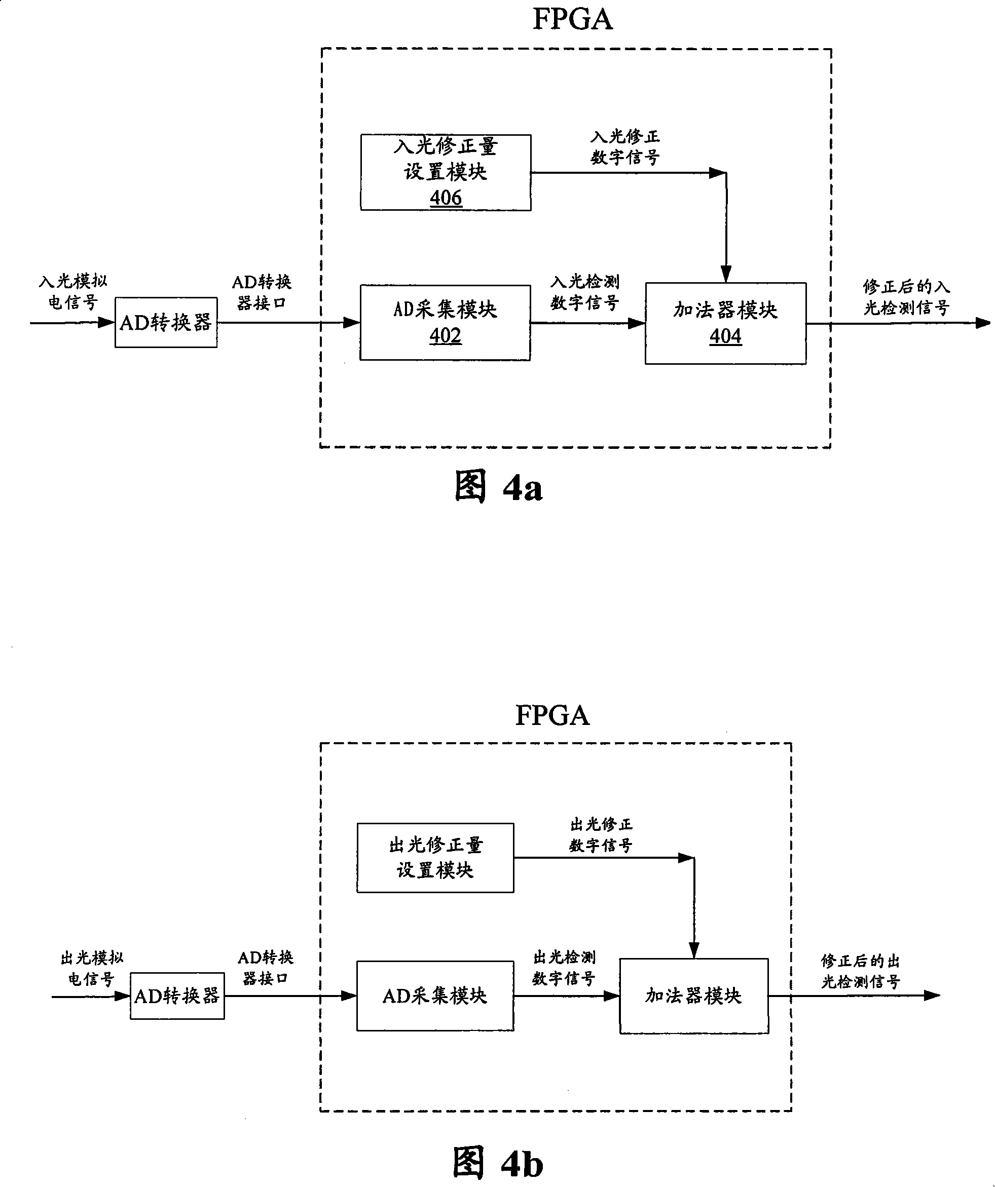
[0057] 4a is a view of a noise compensation circuit realized based on a field programmable gate array (FPGA) according to a third embodiment of the present invention, and FIG. 4b is realized based on a field programmable gate array (FPGA) according to a fourth embodiment of the present invention The view of the noise compensation circuit, the FPGA-b...
no. 3 example
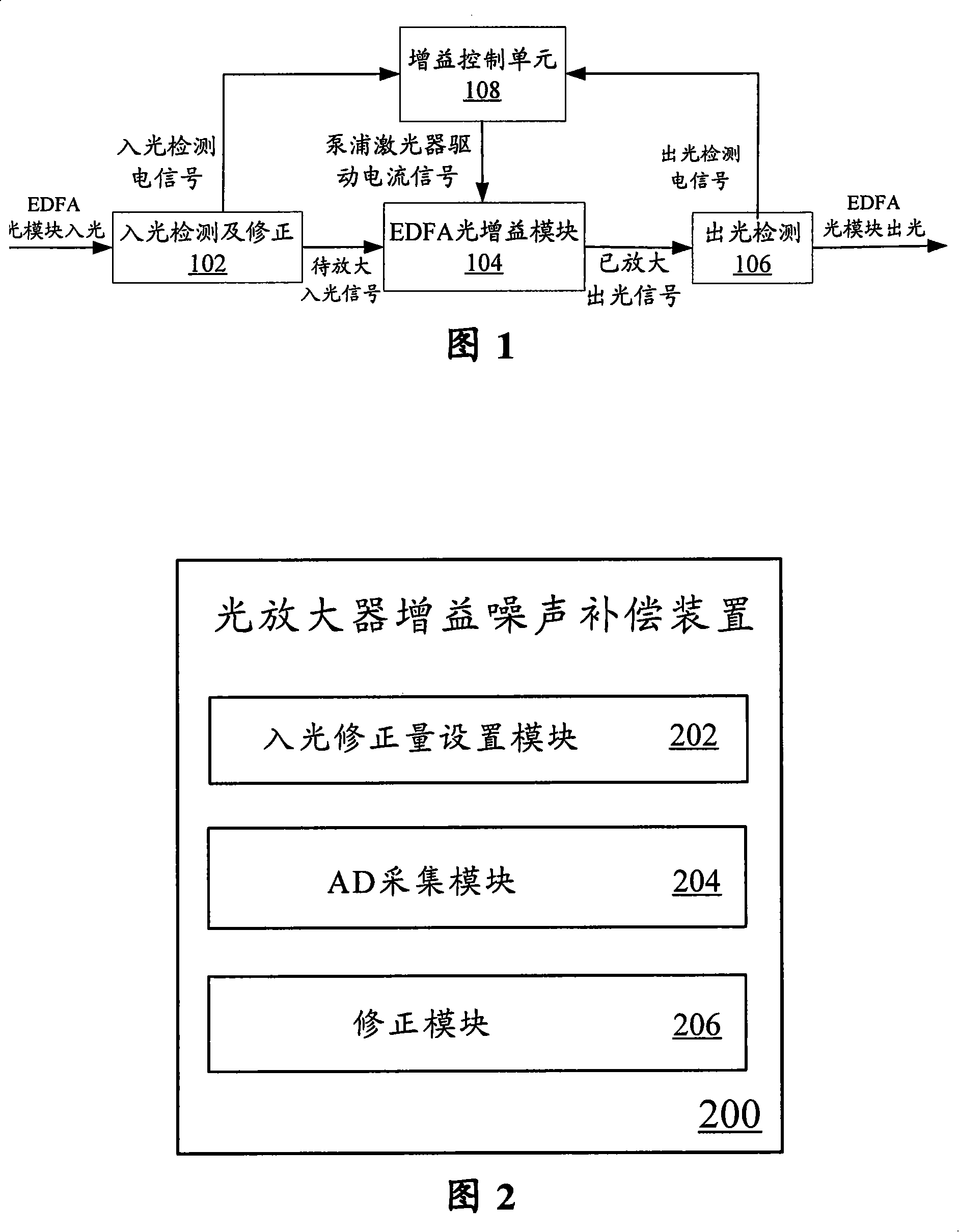
[0060] As shown in Figure 4a, the FPGA realizes the acquisition of the incident light analog electrical signal through the AD acquisition module 402, and the light incident correction amount setting module 406 and the adder module 404 correct the digital signal of the light incident detection and detection, so as to realize the reduction of the ASE noise. compensation function. Gain locking control is performed with the corrected incoming light and the corresponding outgoing light signal as the final equivalent control parameters.
PUM
 Abstract
Description
Claims
Application Information