Surface array semiconductor laser light beam shaping device

A beam shaping and semiconductor technology, applied in the direction of semiconductor lasers, lasers, laser components, etc., can solve the problems of poor beam quality, difficulty in obtaining high-brightness small spots, etc., and achieve the effect of simple structure, convenient adjustment, and easy manufacture

Inactive Publication Date: 2008-03-19
CHANGCHUN INST OF OPTICS FINE MECHANICS & PHYSICS CHINESE ACAD OF SCI
View PDF0 Cites 60 Cited by
  • Summary
  • Abstract
  • Description
  • Claims
  • Application Information

AI Technical Summary

Problems solved by technology

Due to the large difference in the beam quality of the fast and slow axes of the single-tube semiconductor laser, the beam output ...

Method used


Image

  • Surface array semiconductor laser light beam shaping device
  • Surface array semiconductor laser light beam shaping device
  • Surface array semiconductor laser light beam shaping device

Examples


Embodiment Construction

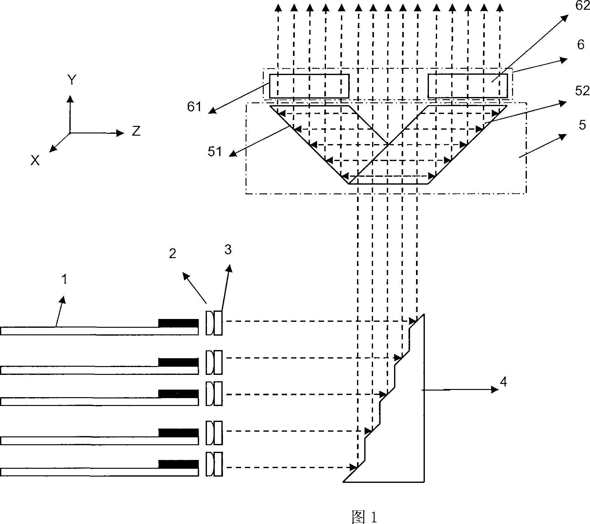
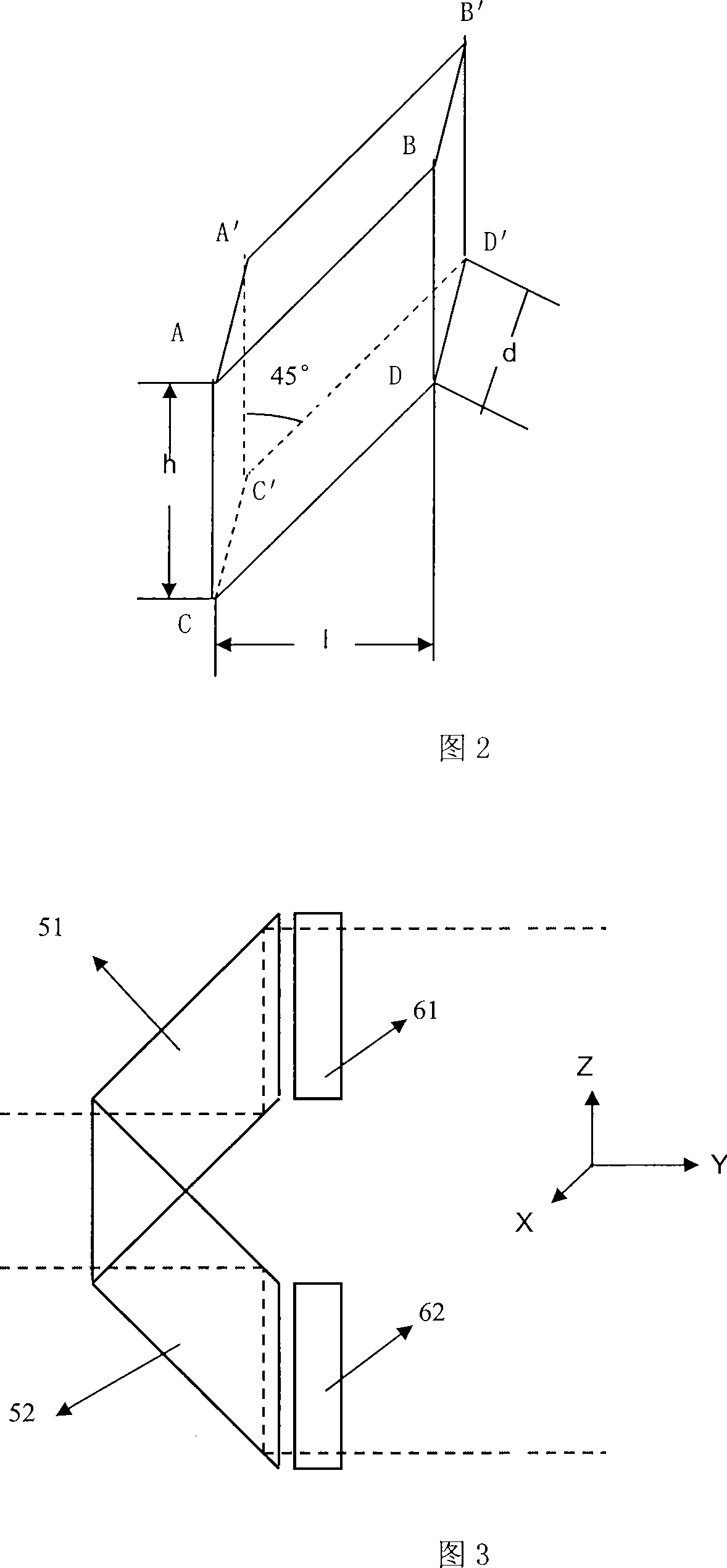
[0019] As shown in Figure 1, the beam shaping device of the area array semiconductor laser of the present invention comprises fast axis collimator mirror 2, slow axis collimator mirror 3, stepped mirror 4, the first parallelepiped prism group 5, the second parallelepiped prism group 6.

[0020] The light beam emitted by the area array semiconductor laser propagates along the Z-axis direction; before the light beam changes direction without step mirror 4, the fast axis direction is the Y-axis direction shown in Figure 1, and the slow axis direction is the X-axis direction shown in Figure 1 After the light beam is changed in direction by the stepped mirror 4, the fast axis direction is the Z-axis direction shown in Figure 1, and the slow axis direction is the X-axis direction shown in Figure 1.

[0021] The fast-axis collimator 2 adopts a cylindrical lens, a semi-cylindrical lens or a graded-index lens; the slow-axis collimator 3 adopts a microcylindrical lens array. The fast-a...


PUM


Abstract

The present invention relates to a beam reshaping device for a plane array semiconductor laser. The device includes a fast axis collimating lens, a slow axis collimating lens, a ladder lens, a first parallelepiped prism unit, and a second parallelepiped prism unit. The beam emitted by the plane array semiconductor laser passes through the fast axis collimating lens and the slow axis collimating lens, and lowers the divergence angle of the fast axis and the divergence angle of the slow axis. The irradiance interspace between bars can be eliminated by the ladder lens and can be compressed in the direction of the fast axis. Finally, part of beam can be moved parallel along the fast axis direction by the first parallelepiped prism unit and the second parallelepiped prism unit, and then be moved along the slow axis direction. Through the above process, the beam is realigned, and the purpose that the quality of the fast axis beam and the quality of the slow axis beam tend to be coincident is reached. The realigned beam can get high-power high-brightness facula after being focused. The optical apparatus used in the present invention is easy to be produced and convenient to be adjusted with simple structure.

Description

technical field [0001] The invention relates to a beam shaping device of a high-power area array semiconductor laser. Background technique [0002] Compared with other types of lasers, semiconductor lasers (LD) have the advantages of small size, light weight, high efficiency, long life, and direct current modulation, so they are widely used in various fields such as industry, medical, military, and communication. However, semiconductor lasers also have inherent defects. The size of the active layer is about 1 μm in the direction perpendicular to the p-n junction plane (fast axis direction), and the beam divergence angle is 30°-60°. In the direction parallel to the p-n junction plane (fast axis direction) The size of the active layer on the slow axis direction) is about 100-200 μm, and the divergence angle is 6-10°. The asymmetry of the beam waist size and the divergence angle of the fast and slow axes makes the beam quality vary greatly, and the output beam also has serious ...

Claims


Application Information

Patent Timeline
IPC IPC(8): G02B27/09G02B3/06H01S5/00
Inventor 冯广智王立军刘云顾媛媛
Owner CHANGCHUN INST OF OPTICS FINE MECHANICS & PHYSICS CHINESE ACAD OF SCI
Why Eureka
Try Eureka