Apparatuses and methods for manipulating droplets on a printed circuit board

A printed circuit board, printed circuit technology, applied in chemical instruments and methods, biochemical equipment and methods, microelectronics and microstructure devices, etc., can solve problems such as low resolution

Inactive Publication Date: 2012-07-04
DUKE UNIV
View PDF3 Cites 0 Cited by
  • Summary
  • Abstract
  • Description
  • Claims
  • Application Information

AI Technical Summary

Problems solved by technology

[0012] In particular, printed circuit board (PCB) technology offers many properties and offers materials similar to traditional semiconductor microfabrication, albeit at very low resolution

Method used


Image

  • Apparatuses and methods for manipulating droplets on a printed circuit board
  • Apparatuses and methods for manipulating droplets on a printed circuit board
  • Apparatuses and methods for manipulating droplets on a printed circuit board

Examples


Embodiment Construction

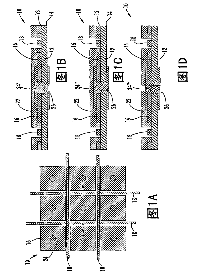
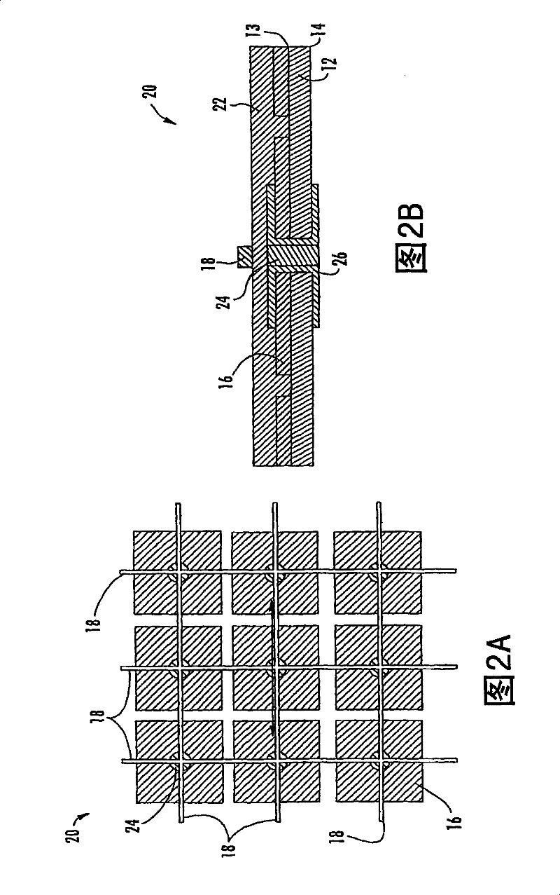
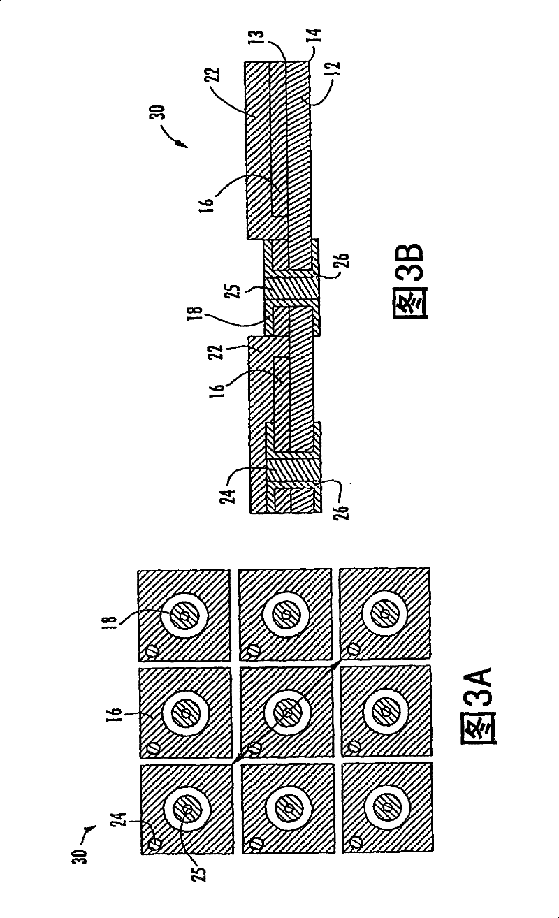
[0104] Having discussed above general embodiments and processes of the present invention, a more specific embodiment of the manufacture of a device for manipulating microvolume liquid samples, wherein the device comprises a printed circuit board substrate, will now be discussed.

[0105] In a preferred embodiment, a 1 / 4 Oz (~9 μm) clad copper. Drill 8mil vias through the substrate. These vias are then plated with copper and filled with solder mask or epoxy. Preferably, the vias are button-plated to a thickness of about 5 μm, with specific vias plated, while the rest of the plate is covered by a mask. Mechanically level the button, then fill the vias with solder mask or non-conductive epoxy. After the vias are processed, a flash plating step is performed to a thickness of less than 5 μm. In cases where unfilled vias are desired, another drilling step can be performed to obtain unfilled holes and, if necessary, electroplating. Temporarily, the designed electrode pattern ...


PUM

PropertyMeasurementUnit
volumeaaaaaaaaaa

Abstract

Apparatuses and methods for manipulating droplets on a printed circuit board (PCB) are disclosed. Droplets are actuated upon a printed circuit board substrate surface by the application of electrical potentials to electrodes defined on the PCB. The use of soldermask as an electrode insulator for droplet manipulation as well techniques for adapting other traditional PCB layers and materials for droplet-based microfluidics are also disclosed.

Description

[0001] related application [0002] This invention is related to U.S. Patent Application Serial No. 10 / 253,342, filed September 24, 2002, and U.S. Provisional Patent Application Serial No. 60 / 648,051, filed January 28, 2005; the disclosure thereof It is hereby incorporated by reference in its entirety. field of invention [0003] The presently disclosed subject matter generally relates to apparatus and methods for performing micromanipulation of liquid droplets on a printed circuit board (PCB) substrate. In particular, the presently disclosed subject matter relates to apparatus and methods for fabricating and operating droplet-based microfluidic systems based on conventional PCB technology in which liquid fluid is driven across the surface of the PCB by applying an electrical potential to electrodes defined on the PCB. drop. The presently disclosed subject matter also describes the use of solder masks as electrode insulators for droplet manipulation, as well as techniques fo...

Claims


Application Information

Patent Timeline
Patent Type & Authority Patents(China)
IPC IPC(8): B01D57/00G01F1/64C25D5/08
CPCH01L21/6715G01N27/447B01L3/502707B01L2300/089B01L2400/0415B01L7/52G05D7/0694B01L2300/0864B81C1/00119B81B2201/058B01L2300/0819B01L2300/12B01F13/0071B01L2300/0645B01L2200/12B01L2300/0867B81B3/0021B01L2300/1827B01L3/502792B01F13/0076B01L2400/0424B01L2200/10C12Q1/6846B01L2300/0663B01L2300/0887Y10T436/2575B01F33/3021B01F33/3031G05D19/00B01L2200/0673G01N27/44769G01N27/44791
Inventor V·K·帕穆拉M·G·波拉克R·B·费尔
Owner DUKE UNIV
Why Eureka
Try Eureka