
Method for controlling transfer single-wall carbon nanotube array structure

A single-walled carbon nanotube, array structure technology, applied in nanostructure manufacturing, nanotechnology, nanotechnology and other directions, can solve the problems of inability to maintain the original structure and low success rate

Inactive Publication Date: 2008-03-26
PEKING UNIV
View PDF0 Cites 20 Cited by
  • Summary
  • Abstract
  • Description
  • Claims
  • Application Information

AI Technical Summary

Problems solved by technology

The existing methods for transferring carbon nanotubes include direct contact method and solution dispersion method, etc. These methods have the defects of low success rate and inability to maintain the original structure.

Method used


Image

  • Method for controlling transfer single-wall carbon nanotube array structure
  • Method for controlling transfer single-wall carbon nanotube array structure
  • Method for controlling transfer single-wall carbon nanotube array structure

Examples


Embodiment 1

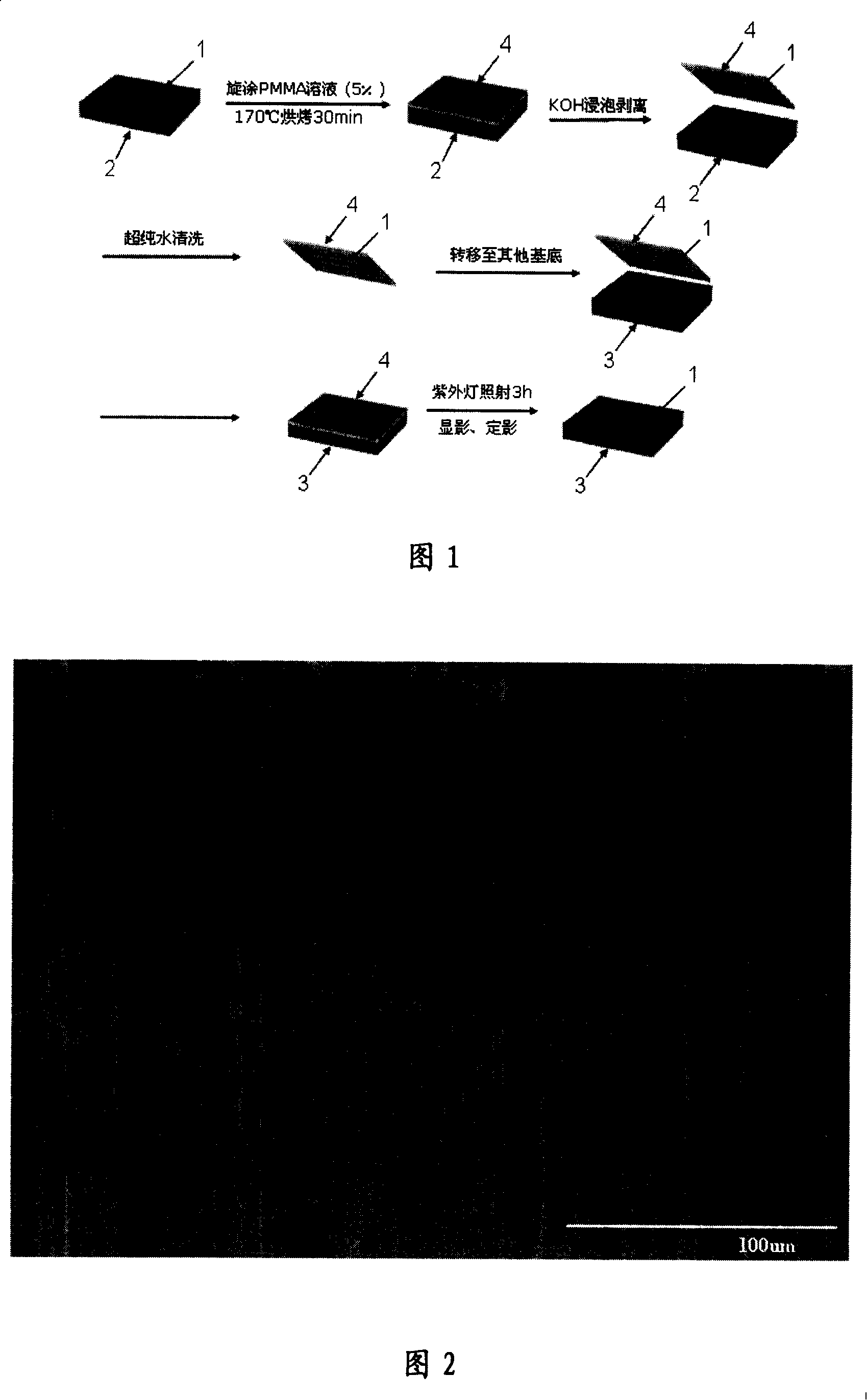
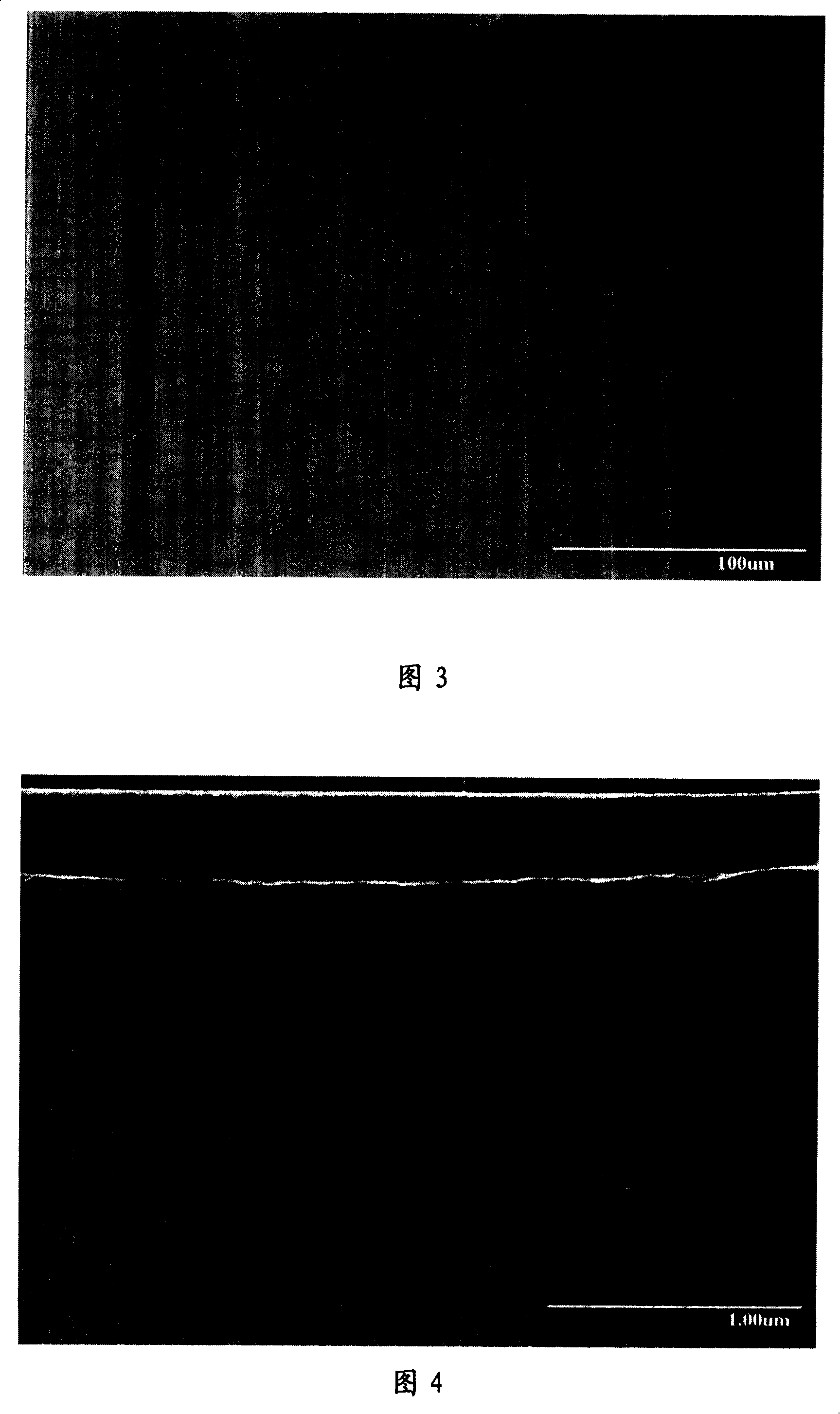
[0026] (1) Using chemical vapor deposition (CVD) on SiO 2 On the surface of the / Si substrate, an array structure of ultra-long parallel single-walled carbon nanotubes with gas flow orientation is grown, as shown in Figure 2;

[0027] (2) the anisole solution of one deck PMMA is spin-coated on its surface, and in 110 ℃ of baking 45 minutes, remove solvent, form PMMA film;

[0028] (3) The SiO covered with PMMA film 2 / Si substrate placed in 1mol·L -1 Heating in the sodium hydroxide solution makes it slightly boil until the PMMA film is separated from the surface and floats;

[0029] (4) Wash the PMMA film with ultrapure water and stick it on another SiO 2 / On the surface of the Si substrate, dry it with high-purity nitrogen and bake it at 110°C for 45 minutes;

[0030] (5) The second piece of SiO with PMMA film on the surface 2 / Si substrate placed under ultraviolet light for 3 hours, and then developed, the PMMA film was removed during the fixing process, and the SiO 2...

Embodiment 2

[0032] (1) Using chemical vapor deposition (CVD) to grow airflow-oriented ultra-long parallel single-walled carbon nanotube array structures on the surface of Si substrates;

[0033] (2) the anisole solution of one deck PMMA is spin-coated on its surface, and in 130 ℃ of baking 40 minutes, remove solvent, form PMMA film;

[0034] (3) Place the Si substrate covered with PMMA film in 2mol L -1 Heating in the sodium hydroxide solution makes it slightly boil until the PMMA film is separated from the surface and floats;

[0035] (4) Wash the PMMA film with ultrapure water, and stick it on the SiO with Pt electrode structure 2 / Si substrate, blow dry with high-purity nitrogen, and bake at 130°C for 40 minutes;

[0036] (5) SiO with a Pt electrode structure with a PMMA film on the surface 2 / Si substrate placed under ultraviolet light for 3 hours, and then developed, the PMMA film was removed during the fixing process, and the ultra-long parallel single-walled carbon nanotube arra...

Embodiment 3

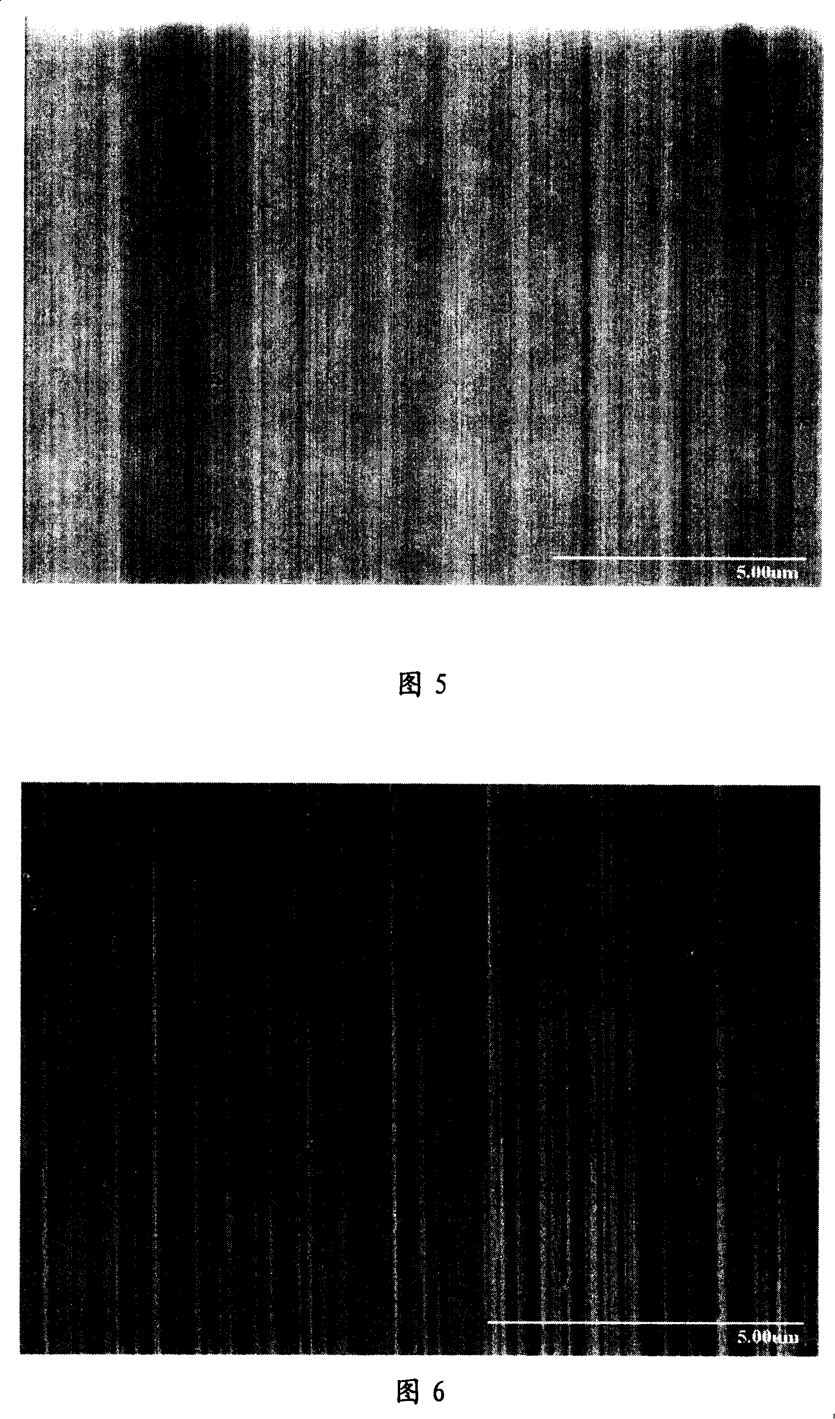
[0038] (1) using chemical vapor deposition (CVD) to grow a single-walled carbon nanotube array structure with a crystal plane orientation on the a crystal plane of the Sapphire substrate, as shown in Figure 5;

[0039] (2) Spin-coat an anisole solution of one deck PMMA on its surface, and bake at 170 DEG C for 30 minutes to remove the solvent to form a PMMA film;

[0040] (3) Place the Sapphire substrate coated with PMMA film in 4mol L -1 Heating in the potassium hydroxide solution makes it slightly boil until the PMMA film is separated from the surface and floats;

[0041] (4) Wash the PMMA film with ultrapure water and stick it on SiO 2 / Si substrate, blow dry with high-purity nitrogen, and bake at 170°C for 30 minutes;

[0042] (5) SiO with PMMA film on the surface 2 / Si substrate placed under ultraviolet light for 3 hours, and then developed, the PMMA film was removed during the fixing process, and the parallel single-walled carbon nanotube array structure grown on the ...


PUM


Abstract

The present invention provides process of controlling the structure of transferred single wall carbon nanotube array and belongs to the field of nanometer structure preparing and processing technology. The process includes the following steps: 1. preparing single wall carbon nanotube array structure on a growth substrate; 2. spin coating polyester solution onto the substrate with single wall carbon nanotube array structure, and stoving in an oven to eliminate solvent and form polyester film; 3. heating in alkali solution to slight boiling to strip the polyester film; 4. washing the polyester film with ultra pure water, adhering the polyester film onto target substrate, blowing to dry with ultra pure nitrogen and roasting in the oven; and 5. exposing, developing and fixing to eliminate polyester film and to obtain transferred single wall carbon nanotube array on the target substrate.

Description

technical field [0001] The invention belongs to the technical field of nanostructure preparation and processing, in particular to a method for controlling and transferring single-walled carbon nanotube array structures. Background technique [0002] Silicon electronic devices are one of the major inventions of the 20th century, and their impact on technology, production, economy and human society is unmatched by any other invention. However, according to Moore's law, the minimum size of silicon-based microelectronics will be 0.08μm in 2011, reaching the physical limit, after which it will be the era of nanoelectronics. Carbon nanotubes have become the most promising next-generation nanoelectronic devices to replace silicon devices due to their excellent electrical and mechanical properties. [0003] For more than ten years, the research on carbon nanotubes has always attracted the attention of the scientific and industrial circles at home and abroad. Experiments have found...

Claims


Application Information

Patent Timeline
Patent Type & Authority Applications(China)
IPC IPC(8): C01B31/02B82B3/00
Inventor 范犇焦丽颖刘忠范张锦张依
Owner PEKING UNIV
Learn More