Method of forming a phase change memory and method for forming phase change layer

一种相变存储器、相变层的技术,应用在制造相变存储器,形成相变存储器中的相变层领域,能够解决GST层沉积温度增加等问题,达到尺寸减小、增加集成度、重置电流减小的效果

Inactive Publication Date: 2008-04-23
SAMSUNG ELECTRONICS CO LTD
View PDF0 Cites 7 Cited by
  • Summary
  • Abstract
  • Description
  • Claims
  • Application Information

AI Technical Summary

Problems solved by technology

[0014] However, when the GST layer is formed using the conventional CVD method, since the organometallic compound including Ge is a tetravalent stable compound, the deposition temperature of the GST layer increases
Therefore, it is difficult to form a GST layer with excellent step coverage to fill a contact hole with a diameter of 100 nm or less

Method used


Image

  • Method of forming a phase change memory and method for forming phase change layer
  • Method of forming a phase change memory and method for forming phase change layer
  • Method of forming a phase change memory and method for forming phase change layer

Examples


Embodiment Construction

[0040] The present invention will now be described more fully with reference to the accompanying drawings, in which exemplary embodiments of the invention are shown. Here, the thicknesses and regions of layers shown in the drawings are exaggerated for clarity.

[0041] First, a method of manufacturing a phase change memory will be described. In addition, a method of manufacturing a phase change layer in a phase change memory will be described simultaneously.

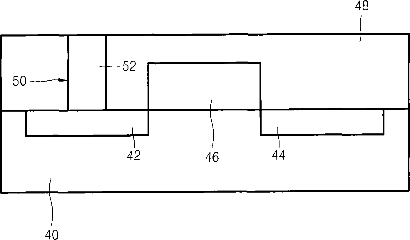
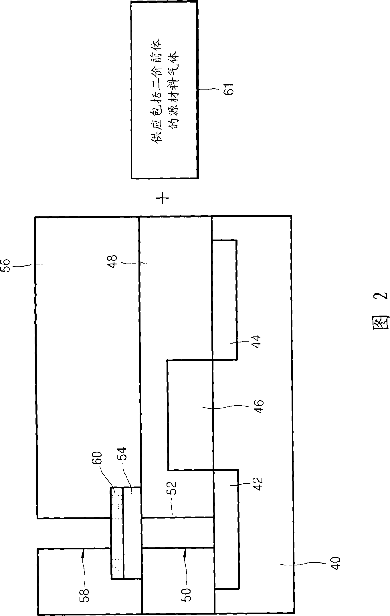
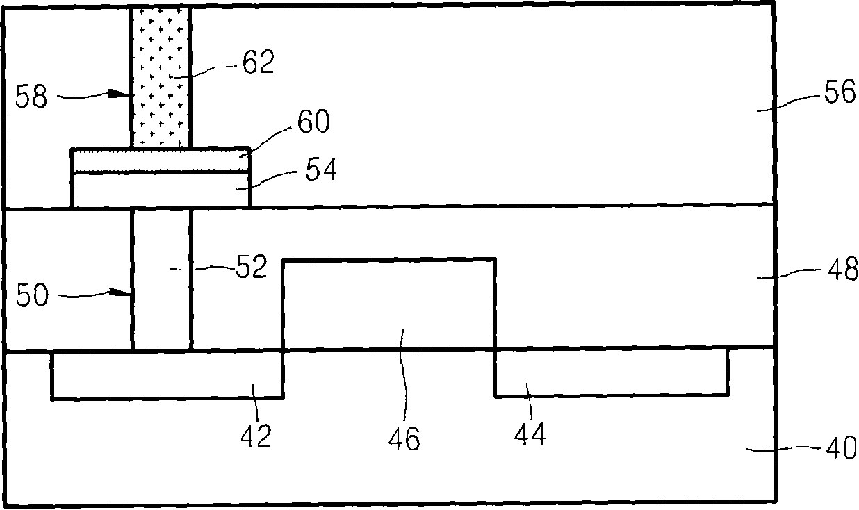
[0042] Figures 1 to 4 is a cross-sectional view illustrating a method of manufacturing a phase change memory according to an embodiment of the present invention. refer to figure 1 A gate stack 46 is formed in a predetermined region of an active region defined by a device isolation layer (not shown) on the p-type or n-type substrate 40 . The gate stack 46 includes a gate insulating layer and a gate electrode. The first impurity region 42 and the second impurity region 44 are formed between the device isolation layer...


PUM


Abstract

A method for manufacturing phase change memory and a method for forming a phase change layer in the phase change memory are provided in the present invention. The method for manufacturing the phase change memory includes providing a bottom layer comprising a germanium (Ge) bivalent first precursor forming the phase change layer onto it. The phase change layer may be formed by one of MVCOD, cyclic-CVD or ALD. The composition of the phase change layer may be varied by modifying the deposition pressure, deposition temperature, and / or supply rate of reaction gas. The deposition pressure may range from about 0.001-10 torr, the deposition temperature may range from about 150-350 DEG C., and the supply rate of the reaction gas may range from about 0-1 slm.

Description

technical field [0001] The present invention relates to a method of manufacturing a semiconductor memory, and more particularly, to a method of manufacturing a phase change memory and a method of forming a phase change layer in the phase change memory. Background technique [0002] The electrical resistance of a phase change material changes depending on whether the phase change material is in a crystalline or amorphous state. That is, the phase change material has two states that are clearly distinguished by the resistance of the phase change material in each of the crystalline state and the amorphous state. The two states of a phase change material change reversibly depending on temperature. [0003] A phase change memory such as PRAM (Phase Change Random Access Memory) includes a phase change layer formed of the above-mentioned phase change material as a means for storing data bits. [0004] A well-known example of a phase change material is Ge 2 Sb 2 Te 5 (GST). ...

Claims


Application Information

Patent Timeline
Patent Type & Authority Applications(China)
IPC IPC(8): H01L45/00
CPCH01L27/2436H01L45/06H01L45/144C23C16/305H01L45/1683H01L45/1616H01L45/1233H10B63/30H10N70/231H10N70/826H10N70/8828H10N70/023H10N70/066
Inventor 申雄澈李在昊姜允善
Owner SAMSUNG ELECTRONICS CO LTD
Why Eureka
Try Eureka