High coupling efficiency composite type two-dimensional photon crystal design method

A technology of two-dimensional photonic crystals and design methods, which is applied in the direction of light guides, optics, optical components, etc., can solve the problems of limited radiated energy, limited directional radiation, and large energy, and achieve reduced reflection loss and directional radiation performance Improvement, far-field divergence angle improvement effect

Inactive Publication Date: 2008-04-30
INST OF OPTICS & ELECTRONICS - CHINESE ACAD OF SCI
View PDF0 Cites 2 Cited by
  • Summary
  • Abstract
  • Description
  • Claims
  • Application Information

AI Technical Summary

Problems solved by technology

[0002] Photonic crystal is a kind of man-made periodic material. Due to its forbidden band characteristics, it can be applied in many aspects. A recent development is to use photonic crystal surface waves to realize directional radiation, and to construct periodic folds on the surface of photonic crystals. The structure can excite the surface mode and couple the surface mode into the radiation mode to achieve directional radiation. The literature proposes that the excitation of the surface wave can be enhanced by improving the coupling efficiency between the waveguide mode and the surface mode, thereby improving the performance of directional radiation; The specific method is to increase the refractive index of the surface cylinder and move the cylinder of the photonic crystal surface forward to form a wrinkled structure, etc. However, only by improving the coupling efficiency between the waveguide mode and the surface mode, the improvement of the directional radiation performance is relatively limited. It has been proposed in the literature that directional radiation can also be achieved by adding point defects to the layer near the exit surface of the photonic crystal to form a resonant mode. However, due to the large energy reflected back to the waveguide by the resonant mode, the radiated energy is greatly limited.

Method used


Image

  • High coupling efficiency composite type two-dimensional photon crystal design method

Examples


Embodiment Construction

[0027] The present invention will be described in detail below in conjunction with the accompanying drawings and specific embodiments, but the scope of protection of the present invention is not limited to the following examples, but should include all content in the claims.

[0028] The concrete process of the embodiment of the present invention is as follows:

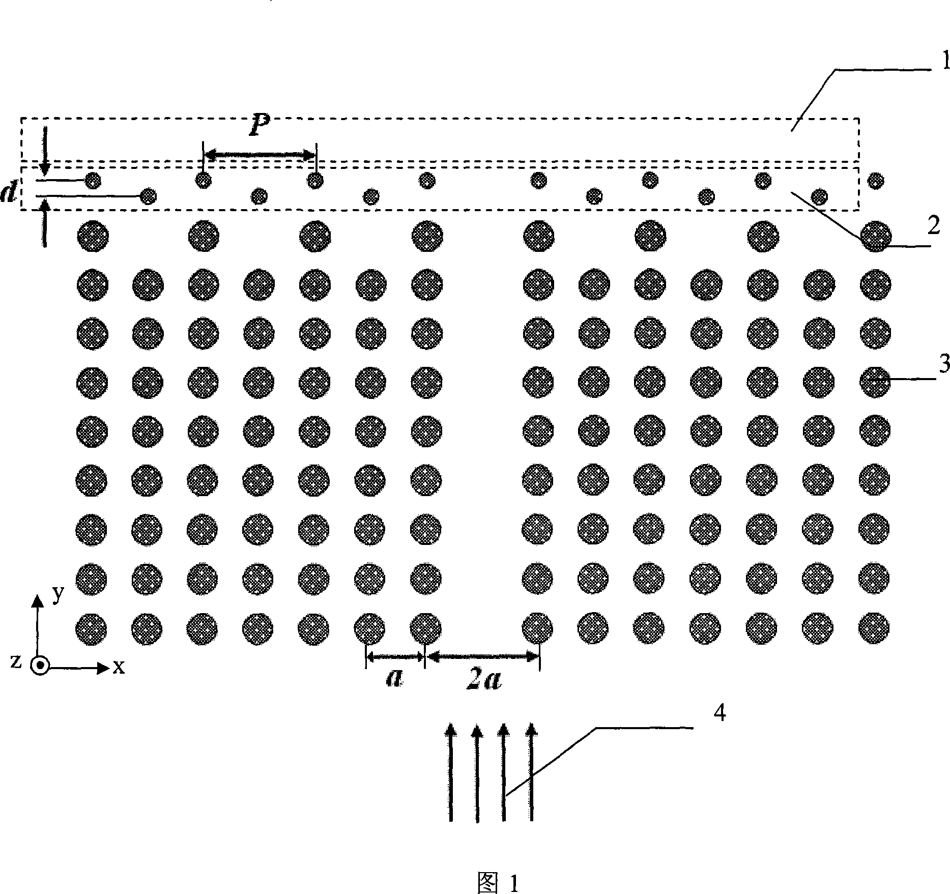
[0029] (1) Determine the wavelength λ=700nm of the incident wave, select gallium arsenide material as the dielectric column material, and air as the background material to carry out the design of the two-dimensional photonic crystal;

[0030] (2) The lattice period of the two-dimensional photonic crystal is a=272nm, the shape of the dielectric column is cylindrical, and its radius is R=0.3a=81.6nm, and the direction perpendicular to the paper surface is the positive direction of the Z axis , the dielectric columns are placed along the Z-axis direction and fixed on the bottom plate on the other side of the Z-axis, wher...


PUM


Abstract

The invention relates to a design method of a compound two-dimensional photon crystal with high coupling efficiency. The invention is characterized in that medium column material and background material of the photon crystal are chosen according to the working wavelength. The crystal lattice cycle of the photon crystal is supposed to be a constant a; and the medium column is arranged and fixed along the z direction which is vertical with a paper face. A photon crystal structure with the length of M * a and the width of N*a is designed. The direction which the long border is arranged at and is taken as an x direction, and the direction which is vertical with the x direction is taken as a y direction. And then the middle position of the photon crystal is taken on the x direction, and all of the medium columns along the y direction at the middle position are lost to form a wave-guide structure. Incidence light incidents the wave-guide structure from the lower part of the photon crystal structure. The section dimension of the medium column of the out emitting layer of the photon crystal is reduced, and the medium columns in even number order in the layer are flatly moved downward to form a folded structure, and the medium columns in even number order on the layer which is lower than the folded layer is taken out to form a defect structure. The excitation of a surface mould can be increased by the structure which is designed in the invention. The energy of directional radiation can be greatly improved. Simultaneously, the astringency of the out emitting beam is also improved.

Description

technical field [0001] The invention relates to a method for improving the coupling efficiency of a photonic crystal by introducing a composite structure, in particular to a design method for a composite two-dimensional photonic crystal with high coupling efficiency. Background technique [0002] Photonic crystal is a kind of artificially manufactured periodic material. Due to its bandgap characteristics, it can be applied in many aspects. A recent development is to use photonic crystal surface waves to realize directional radiation, and to construct periodic folds on the surface of photonic crystals. The structure can excite the surface mode and couple the surface mode into the radiation mode to achieve directional radiation. The literature proposes that the excitation of the surface wave can be enhanced by improving the coupling efficiency between the waveguide mode and the surface mode, thereby improving the performance of directional radiation; The specific method is to ...

Claims


Application Information

Patent Timeline
IPC IPC(8): G02B6/122
Inventor 罗先刚祁云飞杜春雷
Owner INST OF OPTICS & ELECTRONICS - CHINESE ACAD OF SCI
Why Eureka
Try Eureka