A non volatile memory structure and its making method

A non-volatile, memory technology, applied in semiconductor/solid-state device manufacturing, electric solid-state devices, semiconductor devices, etc., can solve the problems of difficult SAB layer removal, complex process control, poor data retention, etc., and achieve simple control and simple process Process, the effect of improving production efficiency

Inactive Publication Date: 2008-04-30
GRACE SEMICON MFG CORP
View PDF0 Cites 5 Cited by
  • Summary
  • Abstract
  • Description
  • Claims
  • Application Information

AI Technical Summary

Problems solved by technology

Since the self-aligned barrier layer (Salicide block, SAB) in the conventional logic process is relatively thin, the memory device manufactured by the conventional logic process has poor data retention
It is known from experiments that a thicker SAB layer can obtain good data retention. However, when the SAB oxide layer reaches a certain thickness, such as more than 1,000 Å, the removal of the SAB layer becomes relatively difficult, and the process control also becomes very complicated

Method used


Image

  • A non volatile memory structure and its making method
  • A non volatile memory structure and its making method

Examples


Embodiment Construction

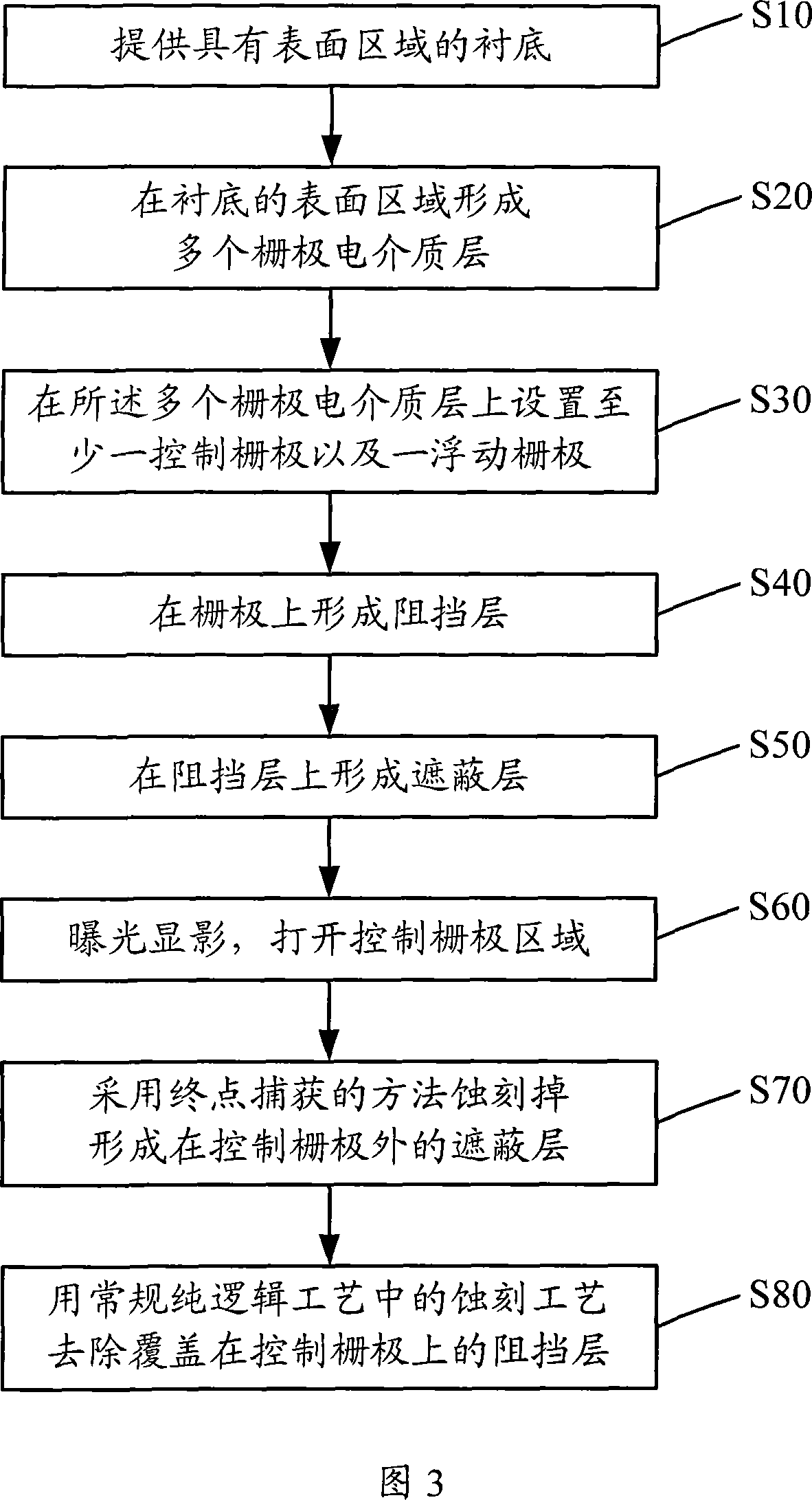
[0015] The non-volatile memory structure and the manufacturing method thereof of the present invention will be described in further detail below with reference to a specific embodiment.

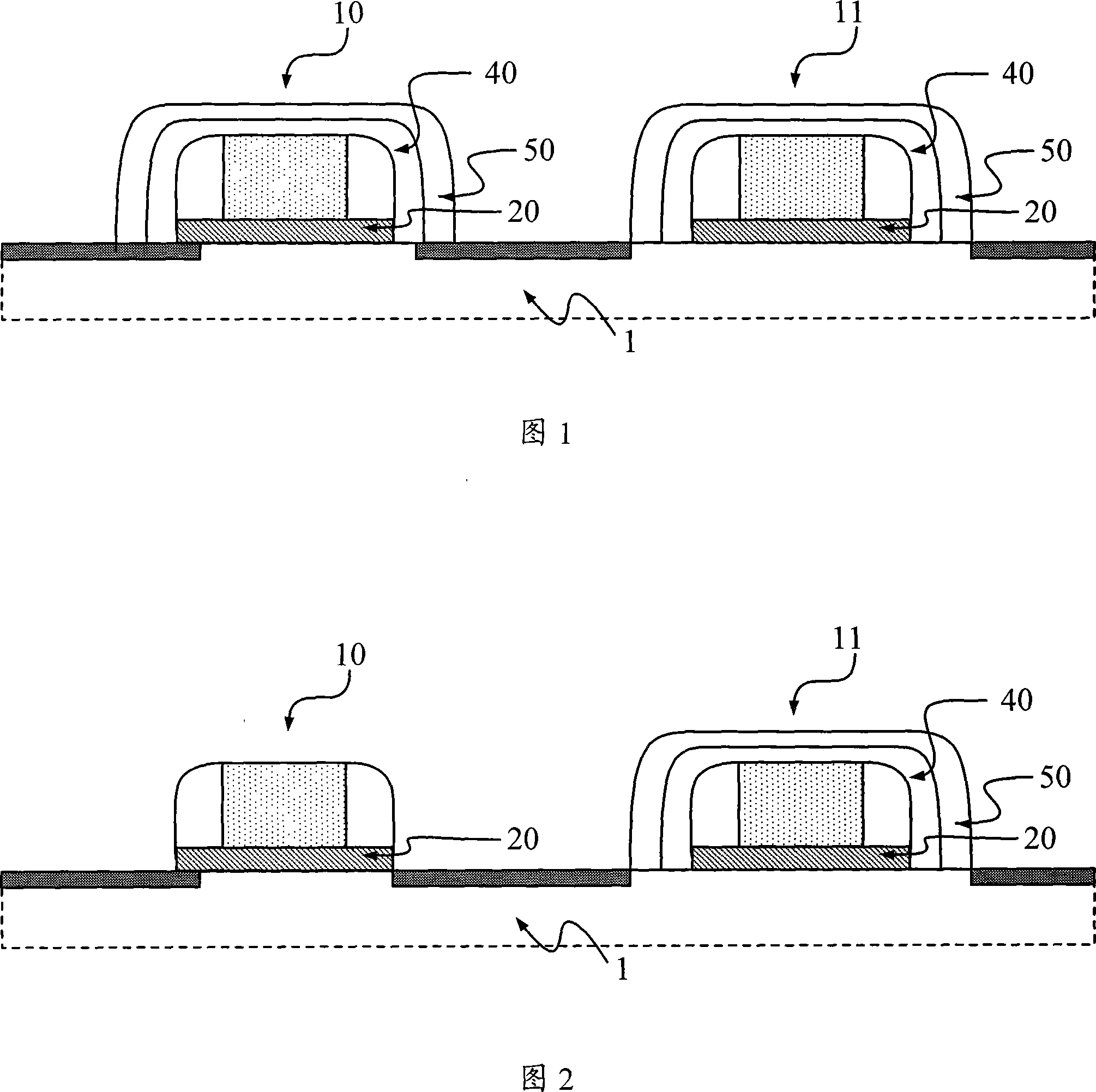
[0016] Please refer to FIG. 1 , which is a schematic cross-sectional view of the structure of the non-volatile memory device before etching the SAB layer according to the present invention. As shown, the non-volatile memory structure of the present invention includes a substrate 1 having a surface area on which a plurality of gate dielectric layers 20 (only two are shown) are formed, and At least one control gate 10 and a floating gate 11 are disposed on each gate dielectric layer 20 , and then a blocking layer 40 and a shielding layer 50 are sequentially covered on the control gate 10 and the floating gate 11 .

[0017] More specifically, the blocking layer 40 is silicon dioxide, and the shielding layer 50 is a silicon nitride layer, and the two layers together constitute a self-aligned bloc...


PUM


Abstract

The invention provides a non-volatile memory structure and a manufacture method thereof. The device includes an underlay with a surface area, which is provided thereon with a plurality of grid dielectric medium layers, wherein, at least two grid dielectric medium layers are provided thereon with a control grid and a floating grid respectively. The control grid and the floating grid are covered by a silicon dioxide barrier layer and a silicon nitride shield layer in turn. The barrier layer and the shield layer co-form a self alignment barrier layer (SAB). The invention has the advantages of good data retentivity, logic process compatibility, simpler process control and efficiency improvement.

Description

technical field [0001] The present invention relates to a semiconductor device structure and a manufacturing method thereof, in particular to a programmable non-volatile device structure and a manufacturing method thereof. Background technique [0002] Logic circuits can achieve good data processing performance, while memory devices can achieve good data retention characteristics. If these two devices are designed on the same circuit, they can achieve good data processing and storage performance at the same time, but correspondingly , the technological process will become relatively complicated and the cost will be high. For some special function devices, such as the driver circuit (Driver) of high-voltage devices, the data required to be stored is not much, and the proportion of the storage device in the entire circuit is small, so the logic process can be used to manufacture such a storage device. [0003] The most critical performance to measure the quality of this stora...

Claims


Application Information

Patent Timeline
Patent Type & Authority Applications(China)
IPC IPC(8): H01L27/115H01L21/8247
Inventor 肖海波
Owner GRACE SEMICON MFG CORP
Why Eureka
Try Eureka