Eureka AIR delivers breakthrough ideas for toughest innovation challenges, trusted by R&D personnel around the world.

Multiple quantum well nitride light emitting diode with carrier supplying layer

A nitride and carrier technology, which can be used in phonon exciters, lasers, laser parts, etc., and can solve problems such as cost and doping of light-emitting layers

Active Publication Date: 2008-05-07
EPISTAR CORP
View PDF1 Cites 5 Cited by
  • Summary
  • Abstract
  • Description
  • Claims
  • Application Information

AI Technical Summary

Problems solved by technology

[0005] In other words, doping impurities in the light-emitting layer of the LED does help to improve the efficiency of carrier recombination, but this improvement comes at a price

Method used


Image

  • Multiple quantum well nitride light emitting diode with carrier supplying layer
  • Multiple quantum well nitride light emitting diode with carrier supplying layer
  • Multiple quantum well nitride light emitting diode with carrier supplying layer

Examples


Embodiment Construction

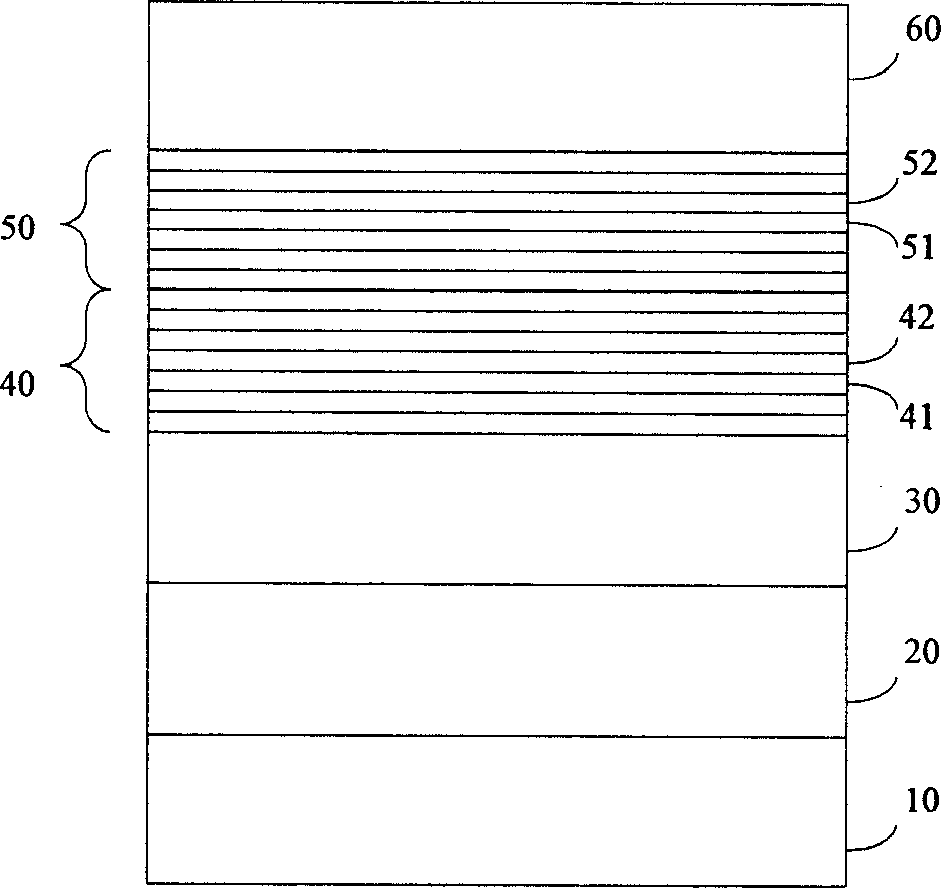
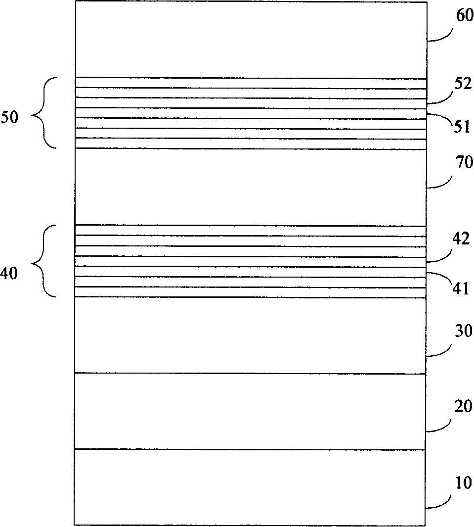
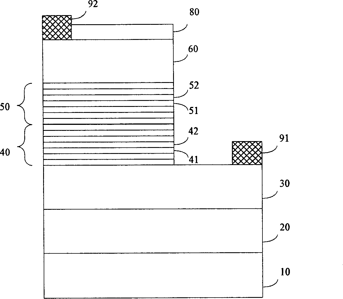
[0023] figure 1 Shown is a schematic diagram of a nitride MQW LED structure according to a first embodiment of the present invention. Please note that this specification uses the term "LED structure" to refer to the epitaxial structure of an LED, and the term "LED device" to refer to the formation of an LED structure, and then through the subsequent chip process (chip process) in the LED A semiconductor device obtained after electrodes are formed on the structure.

[0024] Such as figure 1 As shown, at the bottom of the above-mentioned LED structure, the substrate 10 is usually made of aluminum oxide single crystal (sapphire) or an oxide single crystal with a lattice constant close to that of the epitaxial layer of the LED structure. The substrate 10 can also be made of SiC (6H-SiC or 4H-SiC), Si, ZnO, GaAs, or MgAl 2 o 4 to make. Generally, the most common material for the substrate 10 is sapphire or SiC. On the upper surface of the substrate 10, then formed by Al a Ga...


PUM

PropertyMeasurementUnit
Thicknessaaaaaaaaaa
Electron concentrationaaaaaaaaaa
Thicknessaaaaaaaaaa

Abstract

The present invention provides a structure of a multiplex quantum-well luminous electrode, wherein, a carrier providing layer is arranged at one side of a luminous layer to provide the extra carrier for the luminous layer to take part in the new combination, thereby preventing / reducing the foreign matters in the luminous layer. The carrier providing layer comprises multiplex well layer and position-barrier layer, which are alternatively piled in the thickness of 5 to 300, so that the total thickness of the carrier providing layer is 1 to 500 nm. The well layer and the position-barrier layer are made of the compound semi-conductor AlpInqGa1-pN (p and q are equal to or more than zero, p plus q is equal to or more than zero and is equal to or less than one) mixed with Si or Ge, but each of the well layer and the position-barrier layer has different compositions, wherein, the position-barrier layer is higher than the energy-band gas of the well layer. The electron thickness of the carrier providing layer is between 1*10<17> and 5*10<21> cm<3>.

Description

[0001] invention technical field [0002] The present invention relates to a nitride multiple quantum well light-emitting diode, in particular to a nitride multiple quantum well light-emitting diode with a carrier supply layer, so as to provide additional carriers and avoid / reduce the use of impurities in the light-emitting layer. Background technique [0003] In order to improve the brightness of gallium nitride (GaN)-based light-emitting diodes (LEDs), US Patent No. 5,578,839 discloses a light-emitting layer (or active layer) doped with n-type impurities (such as Si) and / or p-type impurities (such as Mg or Zn, etc.) In x Ga 1-x LED structure made of N (0<x<1) compound semiconductor. The light-emitting layer of this LED structure is sandwiched between a first clad layer made of n-type GaN-based compound semiconductor and a second clad layer made of p-type GaN-based compound semiconductor. The improvement of the brightness of the LED structure is due to the fact that ...

Claims


Application Information

Patent Timeline
IPC IPC(8): H01L33/00H01S5/343H01L33/06H01L33/32
Inventor 武良文简奉任
Owner EPISTAR CORP
Why Eureka
Eureka Blog
Learn More