Silicon chip shallow plow groove isolation etching method

A technology of shallow trenches and silicon wafers, applied in the manufacture of electrical components, semiconductor/solid-state devices, circuits, etc., can solve the problems of high price of CH2F2 gas, complicated tail gas treatment process, and increased consumption cost, and achieve low cost and step-by-step Less, smooth transition effect

Active Publication Date: 2008-05-14
BEIJING NAURA MICROELECTRONICS EQUIP CO LTD
View PDF0 Cites 56 Cited by
  • Summary
  • Abstract
  • Description
  • Claims
  • Application Information

AI Technical Summary

Problems solved by technology

[0013] However, the disadvantage of this technology is that the price of CH2F2 gas used in the SiO2 layer etching step is relatively high, the tail gas treatment process is more complicated, and special equipment is requ

Method used


Image

  • Silicon chip shallow plow groove isolation etching method
  • Silicon chip shallow plow groove isolation etching method
  • Silicon chip shallow plow groove isolation etching method

Examples


Embodiment Construction

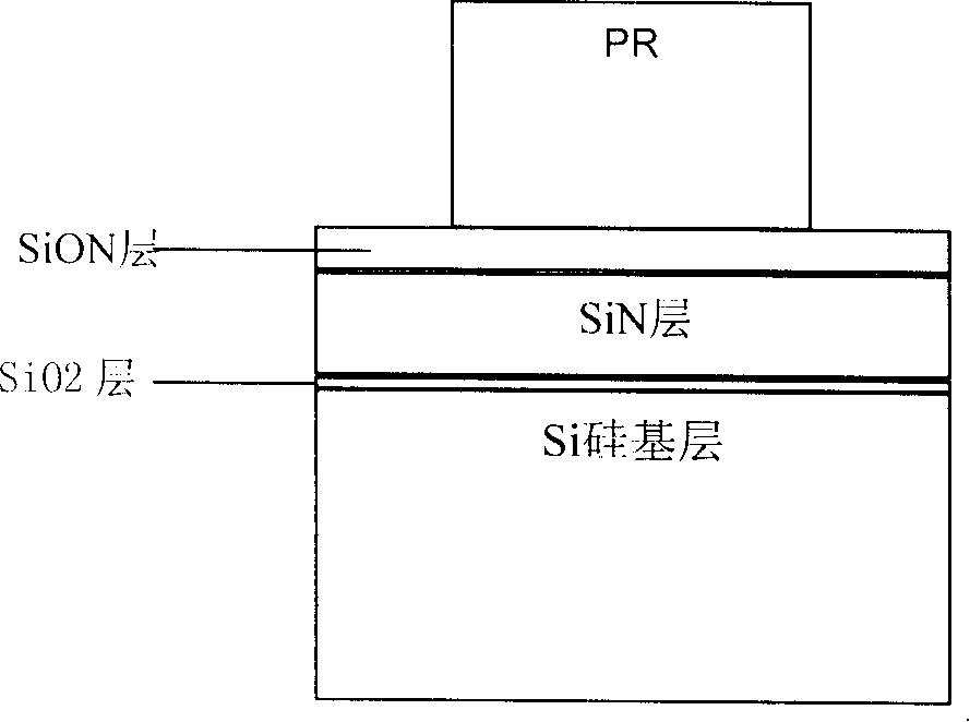
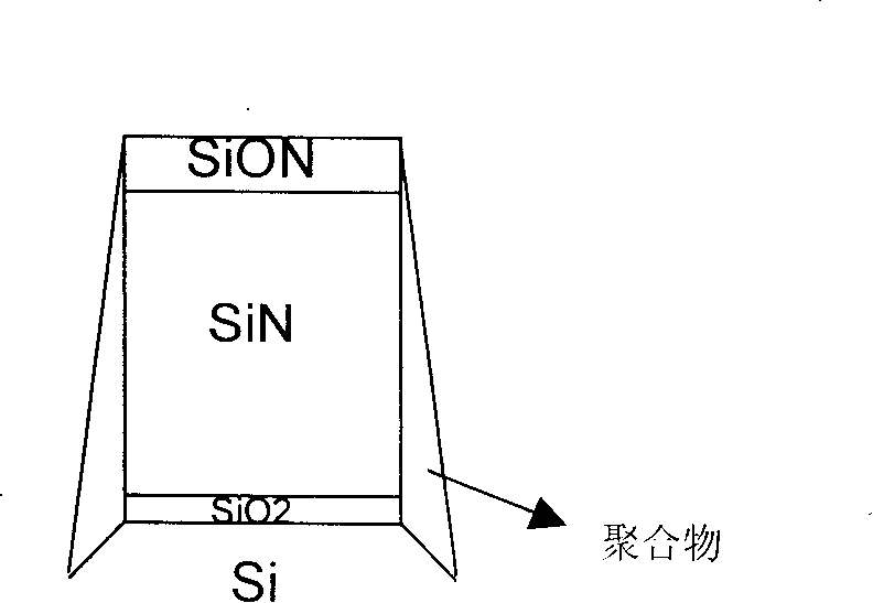
[0035] The method for silicon wafer shallow trench isolation etching of the present invention is mainly used for etching trenches on silicon wafers, such as figure 1 As shown, the silicon wafer is a multi-layer structure, including a silicon upper layer and a silicon base layer, and an oxide layer is arranged between the silicon upper layer and the silicon base layer. The silicon upper layer here mainly includes a SiON (hard mask) layer and a SiN layer. There is an SiO2 oxide layer between the silicon upper layer and the silicon base layer. In the process of performing shallow trench isolation etching on the semiconductor silicon wafer, it is necessary to form a smooth upper part at the junction of the SiO2 layer and the silicon base layer on the side wall of the trench. The rounded corners are conducive to the release of stress and avoid the generation of parasitic conductive channels in the semiconductor silicon wafer.

[0036] The method for silicon wafer shallow trench iso...


PUM


Abstract

The invention discloses a silicon chip shallow trench isolation etching method which is used for etch groove on silicon. The method comprises the following steps: A. upper layer silicon etching step; B. oxide layer etching step, which is used for etching the oxide layer between upper layer silicon and base silicon and is also used for etching partial base silicon for the top fillet etching preparation; C. base silicon etching step which is used for etching groove on silicon base and to form slippery top fillet at the junctional position of oxide layer and silicon base on the sidewall of groove. The etching process gas used in the Step B is mixed gas consisting of HBr gas and CHF3 gas. The etching process gas is ionized into active groups like Br*, CHF*, etc., and can form the top fillet during Step C. The method has the advantages of simple process with less steps, low cost and slippery top fillet formation of etching groove, and is applicable to shallow trench isolation etching and other etchings of various type of semiconductor silicon wafers.

Description

technical field [0001] The invention relates to a semiconductor silicon chip processing technology, in particular to a silicon chip shallow trench isolation etching process. Background technique [0002] At present, microelectronic technology has entered the era of VLSI and system integration, and microelectronic technology has become the symbol and foundation of the entire information age. [0003] In microelectronics technology, to manufacture an integrated circuit, it needs to go through several processes such as integrated circuit design, mask manufacturing, raw material manufacturing, chip processing, packaging, and testing. In this process, etching the semiconductor silicon wafer to form process trenches is the key technology. [0004] Semiconductor silicon wafers generally have a multi-layer structure, including a silicon upper layer and a silicon base layer. The upper silicon layer here mainly includes a SiON (hard mask) layer and a SiN layer. There is an SiO2 oxide...

Claims


Application Information

Patent Timeline
IPC IPC(8): H01L21/762
Inventor 霍秀敏
Owner BEIJING NAURA MICROELECTRONICS EQUIP CO LTD
Why Eureka
Try Eureka