Double phosphorescent coloring agent common adulterate white light organic electroluminescent device and method for fabricating the same

A technology for electroluminescent devices and phosphorescent dyes, which is applied in the fields of electro-solid devices, chemical instruments and methods, semiconductor/solid-state device manufacturing, etc., to achieve the effect of ensuring spectral stability

Inactive Publication Date: 2008-05-14
CHANGZHOU INST OF ENERGY STORAGE MATERIALS &DEVICES
View PDF2 Cites 15 Cited by
  • Summary
  • Abstract
  • Description
  • Claims
  • Application Information

AI Technical Summary

Problems solved by technology

However, judging from the current research, white light organic devices are still far from large-scale commercial applications, and the existing problems are more prominent

Method used


Image

  • Double phosphorescent coloring agent common adulterate white light organic electroluminescent device and method for fabricating the same
  • Double phosphorescent coloring agent common adulterate white light organic electroluminescent device and method for fabricating the same
  • Double phosphorescent coloring agent common adulterate white light organic electroluminescent device and method for fabricating the same

Examples


Embodiment 1

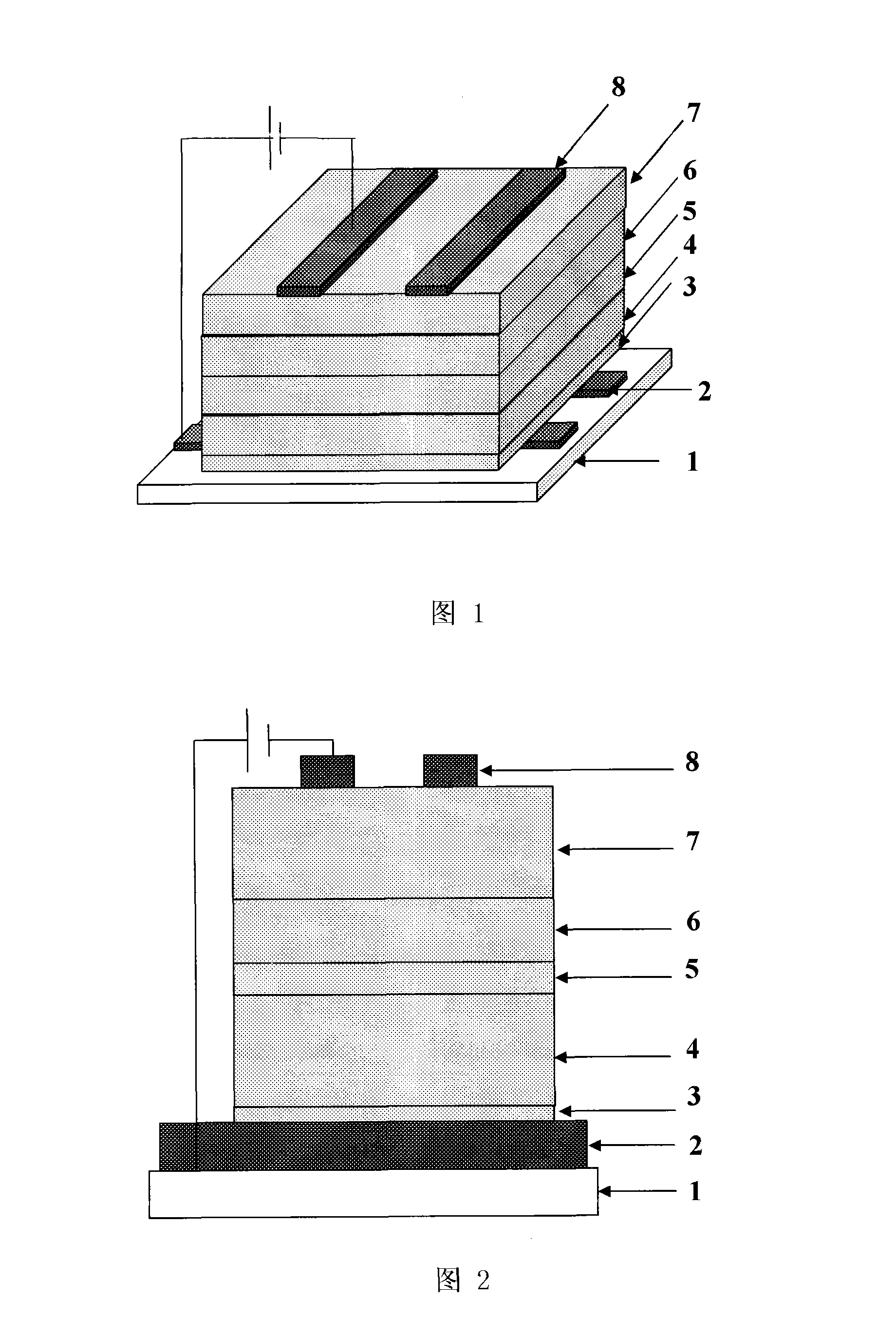
[0030] The ITO on ITO glass was first photolithographically formed into electrodes 4 mm wide and 30 mm long, then cleaned, blown dry with nitrogen, and treated with oxygen plasma for 2 min. 1 to 5 x 10 in vacuum -4 In the coating system of Pa, V is sequentially deposited on the ITO electrode 2 O 5 Vanadium pentoxide hole injection layer, NPB hole transport layer, TCTA electron blocking layer, FIrpic and (fbi) 2 The light-emitting layer composed of Ir(acac) co-doped in mCP, the TAZ electron transport layer, and the composite cathode composed of LiF and metal Al, the two electrodes intersect each other to form the light-emitting area of ​​the device, and the area of ​​the light-emitting area is 16 square millimeters. The thickness of LiF in the metal cathode layer is 1 nm, the thickness of Al is 100 nm, and the metal oxide V 2 O 5 The thickness of the NPB, TCTA, mCP, and TAZ layers is 80, 5, 20, and 40 nm, respectively, and the total thickness of these organic layers is 145 ...

Embodiment 2

[0032] The ITO on ITO glass was first photolithographically formed into electrodes 4 mm wide and 30 mm long, then cleaned, blown dry with nitrogen, and treated with oxygen plasma for 2 min. 1 to 5 x 10 in vacuum -4 In the coating system of Pa, V is sequentially deposited on the ITO electrode 2 O 5 Vanadium pentoxide hole injection layer, NPB hole transport layer, TCTA electron blocking layer, FIrpic and (fbi) 2 The light-emitting layer composed of Ir(acac) co-doped in mCP, the TAZ electron transport layer, and the composite cathode composed of LiF and metal Al, the two electrodes intersect each other to form the light-emitting area of ​​the device, and the area of ​​the light-emitting area is 16 square millimeters. The thickness of LiF in the metal cathode layer is 1 nm, the thickness of Al is 200 nm, and the metal oxide V 2 O 5 The thickness of the NPB, TCTA, mCP, and TAZ layers is 80, 7.5, 20, and 40 nm, respectively, and the total thickness of these organic layers is 14...

Embodiment 3

[0034] The ITO on ITO glass was first photolithographically formed into electrodes 4 mm wide and 30 mm long, then cleaned, blown dry with nitrogen, and treated with oxygen plasma for 2 min. 1 to 5 x 10 in vacuum -4 In the coating system of Pa, MoO is sequentially evaporated on the ITO electrode 3 Molybdenum trioxide hole injection layer, NPB hole transport layer, TCTA electron blocking layer, FIrpic and (fbi) 2 The light-emitting layer composed of Ir(acac) co-doped in mCP, the TAZ electron transport layer, and the composite cathode composed of LiF and metal Al, the two electrodes intersect each other to form the light-emitting area of ​​the device, and the area of ​​the light-emitting area is 16 square millimeters. The thickness of LiF in the metal cathode layer is 1 nm, the thickness of Al is 200 nm, and the thickness of metal oxide MoO 5 The thickness of the NPB, TCTA, mCP, and TAZ layers is 60, 10, 20, and 40 nm, respectively, and the total thickness of these organic laye...


PUM

PropertyMeasurementUnit
thicknessaaaaaaaaaa
thicknessaaaaaaaaaa
thicknessaaaaaaaaaa

Abstract

The invention pertains to double phosphorescent dyes co-doped white organic light-emitting device and discloses the preparation method. The invention adopts sandwich structure and intermingles the two high-efficient phosphorescent dyes together in the wide band gap body; and also takes use of the energy difference between emission layer and its bilateral function layers to form a structure of energy sink type; restricts exaction within the structure completely, thereby realizing composite luminescence. The structure of the device is indium tin oxide (ITO)/metal oxide/hole-transporting layer/electron blocking layer/emission layer composed of the co-doped blue and orange light phosphorescent dyes/electron transporting(hole blocking)layer/metal cathode. The prepared devices are driven by direct voltage and obtain high-efficient white light emission. The maximum electroluminescence current efficiency is 52.8cd/A; the maximum electroluminescence (EL) power efficiency is 42.5lm/W; the maximum luminance is19500 cd/m2. The devices show simultaneous emission of complementary colors of orange and blue and stable spectrum when at work. The device has simple manufacturing process, low cost and excellent stability.

Description

technical field [0001] The invention relates to a white light organic electroluminescence device co-doped with double phosphorescent dyes and a preparation method thereof. Background technique [0002] Organic electroluminescence display is regarded as the most popular emerging display technology in the flat panel display industry and has been extensively studied. Compared with inorganic electroluminescent devices, organic electroluminescent devices have a wide range of material selection, can realize full-color display from blue light region to red light region, low driving voltage, high luminous brightness and luminous efficiency, wide viewing angle, and response speed. Fast, simple manufacturing process, low cost, and easy to achieve large-area and flexible display and many other advantages, so it has developed rapidly in the past 20 years. At present, the research in the field of organic light-emitting display devices has not been limited to academia. Almost all interna...

Claims


Application Information

Patent Timeline
Patent Type & Authority Applications(China)
IPC IPC(8): H01L51/50H01L51/54H01L51/56C09K11/06
CPCY02B20/181Y02B20/00
Inventor 马东阁王琦张智强代岩峰王利祥丁军桥吕剑虹
Owner CHANGZHOU INST OF ENERGY STORAGE MATERIALS &DEVICES
Why Eureka
Try Eureka