Eureka AIR delivers breakthrough ideas for toughest innovation challenges, trusted by R&D personnel around the world.

Test circuit of on-chip multicore processor and design method of testability

A multi-core processor and test circuit technology, applied in the direction of measuring electricity, measuring electrical variables, instruments, etc., can solve the problems of different test excitation and response vectors, increase test overhead and cost, prolong chip test time, etc., to reduce extra costs. Power consumption overhead, reduced test cost, and the effect of shortened test time

Active Publication Date: 2008-05-21
INST OF COMPUTING TECHNOLOGY - CHINESE ACAD OF SCI
View PDF0 Cites 27 Cited by
  • Summary
  • Abstract
  • Description
  • Claims
  • Application Information

AI Technical Summary

Problems solved by technology

However, the data path bandwidth of the on-chip multi-core processor is determined by the characteristics of the working mode, so there may be a mismatch between the data path bandwidth that can be connected to the core and the number of internal scan chains of the core core to be tested, resulting in the waste of the on-chip data path, thus Brings additional test data communication overhead, thereby prolonging the test time of the entire chip and increasing the power consumption of the chip test
[0008] 3. In traditional testing, the test stimuli and response vectors of each part of the chip structure are different, so that each part of the chip needs to be specially transmitted test stimuli and output test responses
However, on-chip multi-core processors have many isomorphic components (such as cores, memories, etc.). Output: input and output system) data transmission speed and bandwidth generate higher requirements, resulting in increased test overhead and cost

Method used


Image

  • Test circuit of on-chip multicore processor and design method of testability
  • Test circuit of on-chip multicore processor and design method of testability
  • Test circuit of on-chip multicore processor and design method of testability

Examples


Embodiment 1

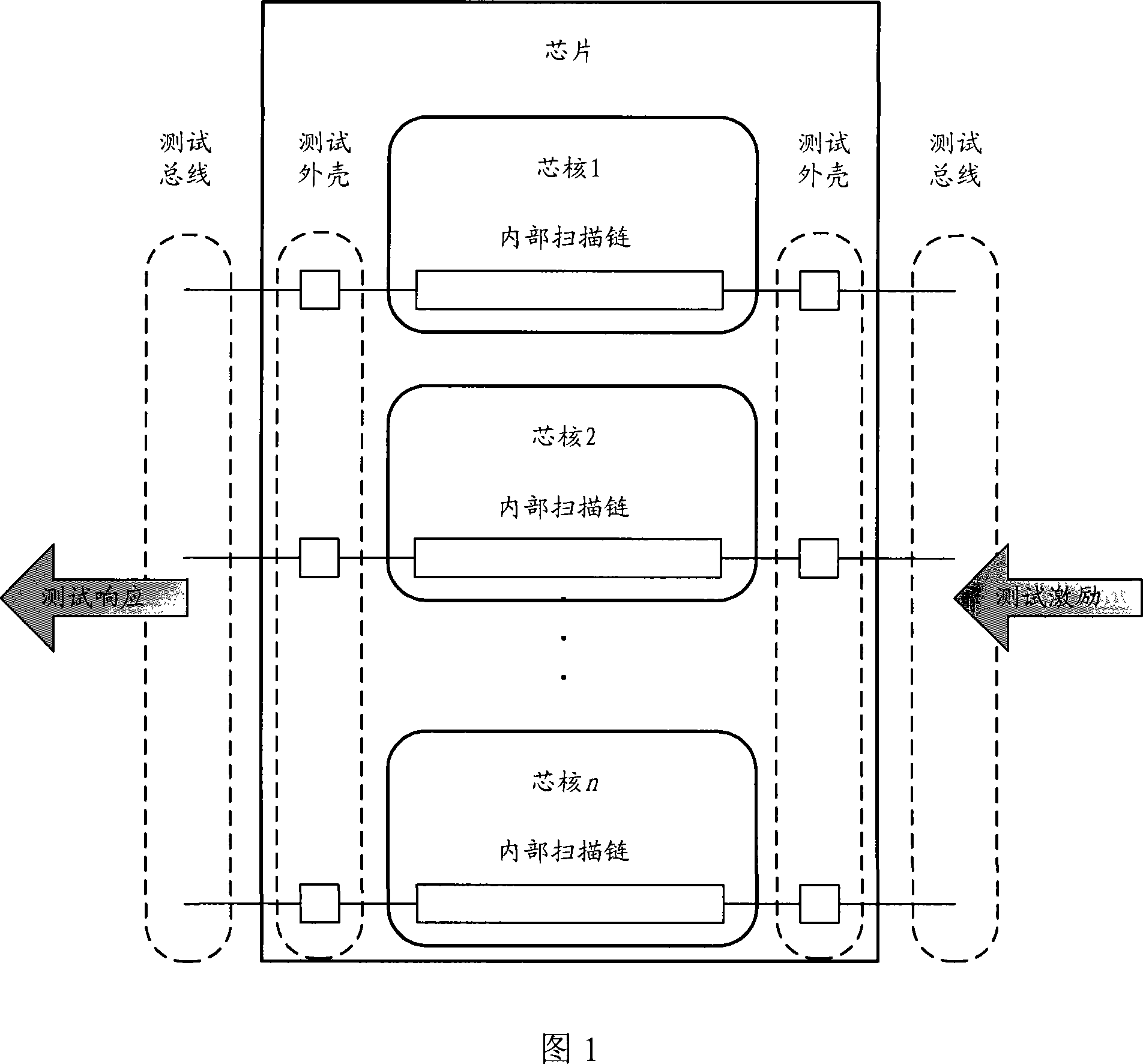
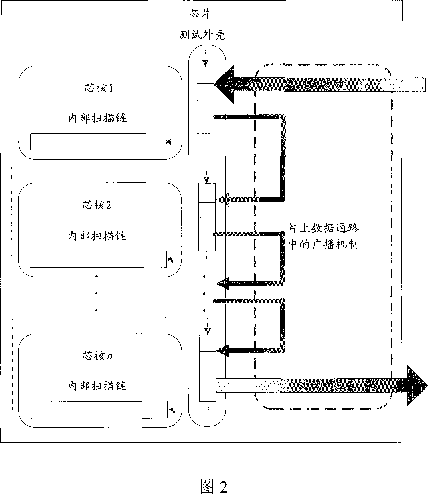
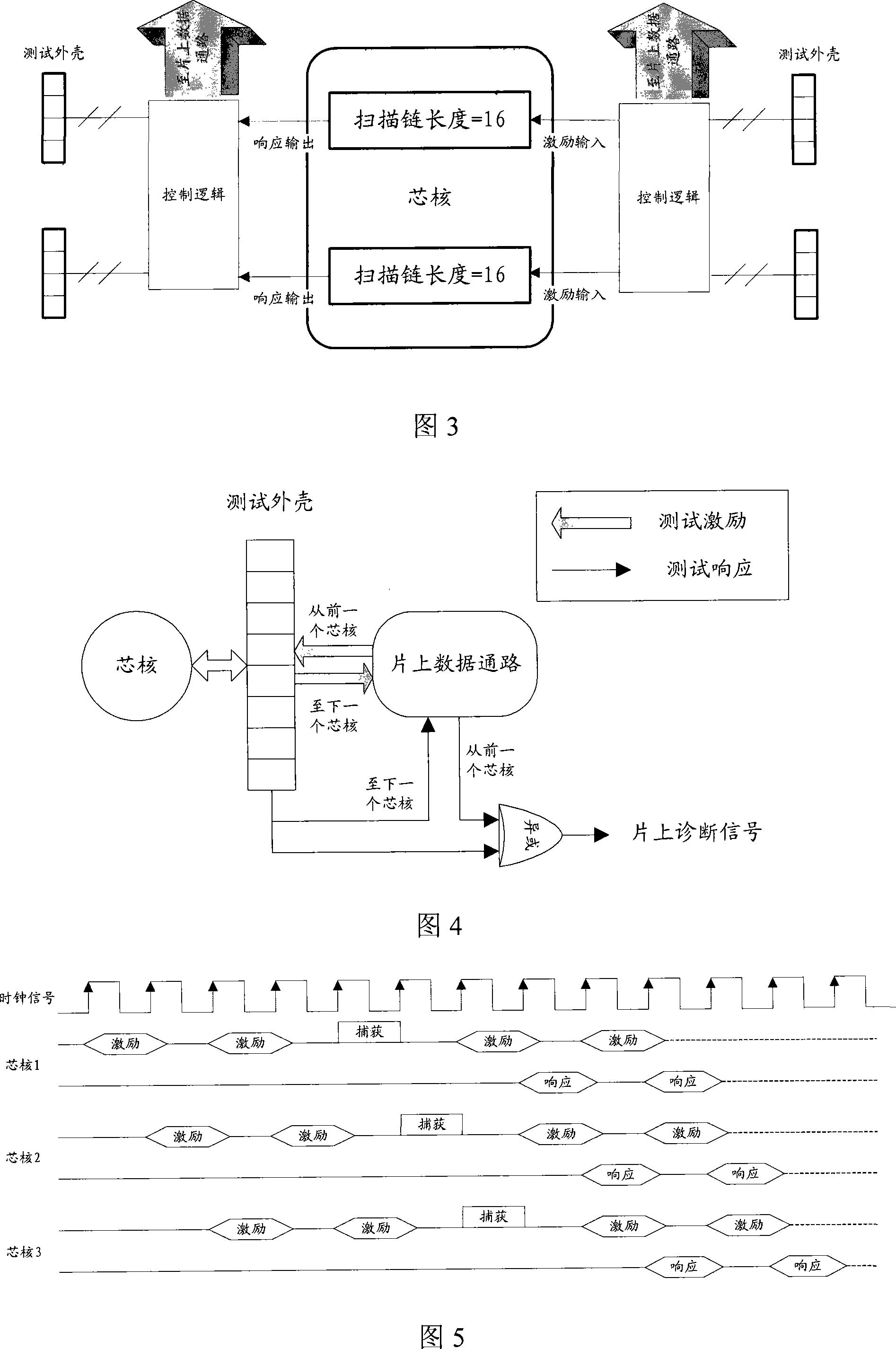
[0046] As shown in Figure 2, Figure 2 is a schematic diagram of the testability design scheme for the on-chip multi-core processor provided by the present invention, and the circuit includes two components: at least one test shell register for buffering core test data to be tested chain, and the interconnection circuit between the test shell register chain and the core core to be tested and the on-chip data path.

[0047] Among them, the test shell register chain used for caching the core test data to be tested is generally divided into multiple groups, and the specific number of groups is determined by the core scanning structure. The determination method will be described in detail below and omitted here temporarily. The test shell register chain is composed of a plurality of registers connected in series, through the interconnection circuit between the test shell register chain and the core core to be tested, and the interconnection circuit between the test shell register ch...


PUM


Abstract

The present invention provides a testing circuit and a testability design method thereof for an on-chip multinuclear processor; wherein, the testing circuit comprises a testing shell register chain, a chip core connecting circuit waiting to be tested, an on-chip data path connecting circuit and a control logic circuit. The chip core connecting circuit waiting to be tested is an interconnection circuit, which is connected between the testing shell register chain and the chip core waiting to be tested. The on-chip data path connecting circuit is the interconnection circuit which is connected between the testing shell register chain and the on-chip data path. The control logic circuit controls the data flow direction of the chip core connecting circuit waiting to be tested and the on-chip data path connecting circuit. The present invention conducts an optimum design according to the characteristics of the on-chip multinuclear processor. The bandwidth of the on-chip data path is fully used. The testing cost is reduced and the amount of a transmission data packet in the on-chip data path is reduced. So an extra power spending caused by mass active data packet is greatly reduced and the testing time is greatly shortened.

Description

technical field [0001] The invention belongs to the technical field of testability design of large-scale integrated circuit chips, in particular, the invention relates to a test case circuit and a design method thereof. Background technique [0002] With the driving of applications and the advancement of technology and materials, the system structure of high-performance computing is facing another major change. ITRS (International Technology Roadmap for Semiconductors: International Technology Roadmap for Semiconductors) predicts that in order to further improve circuit integration and performance, device size, transistor threshold voltage and oxide thickness will be further reduced to meet future development needs. These changes will increase the leakage current exponentially and bring about large deviations in on-chip and inter-chip device parameters. The number of devices per chip will rise from about 200 million to tens of billions in the next ten years. [0003] Tradi...

Claims


Application Information

Patent Timeline
IPC IPC(8): G01R31/3185
Inventor 李佳胡瑜李晓维
Owner INST OF COMPUTING TECHNOLOGY - CHINESE ACAD OF SCI
Why Eureka
Eureka Blog
Learn More