Mask read-only memory and its manufacturing method

A mask read-only, memory technology, applied in the field of memory, can solve the problems of reduced readout speed, difficulty in proportional reduction, etc., and achieve the effect of small bit line spacing, improved readout speed, and small bit line width

Inactive Publication Date: 2008-06-11
GRACE SEMICON MFG CORP
View PDF0 Cites 12 Cited by
  • Summary
  • Abstract
  • Description
  • Claims
  • Application Information

AI Technical Summary

Problems solved by technology

[0006] The object of the present invention is to provide a mask read-only memory and its manufacturing method, which can overcome the problems of diffi

Method used


Image

  • Mask read-only memory and its manufacturing method
  • Mask read-only memory and its manufacturing method
  • Mask read-only memory and its manufacturing method

Examples


Embodiment Construction

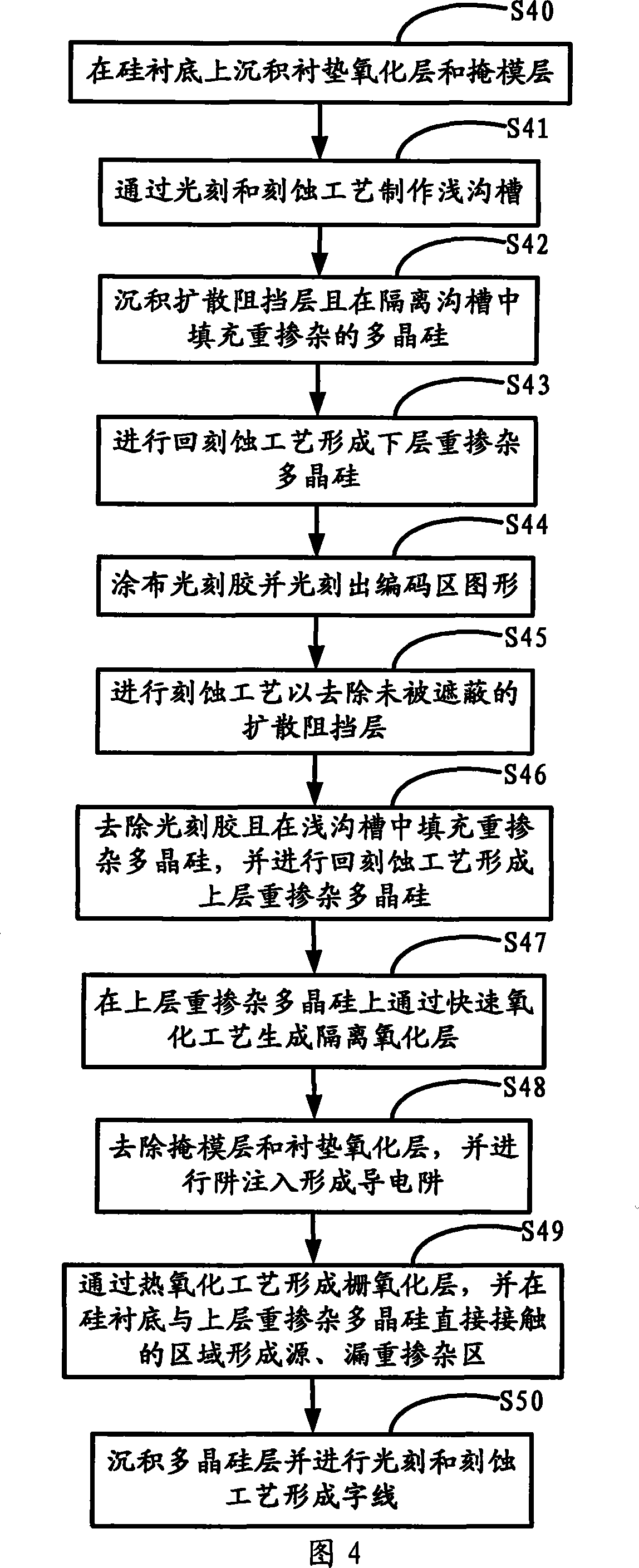
[0027] The photolithography method of the present invention that can improve the pattern quality will be further described in detail below.

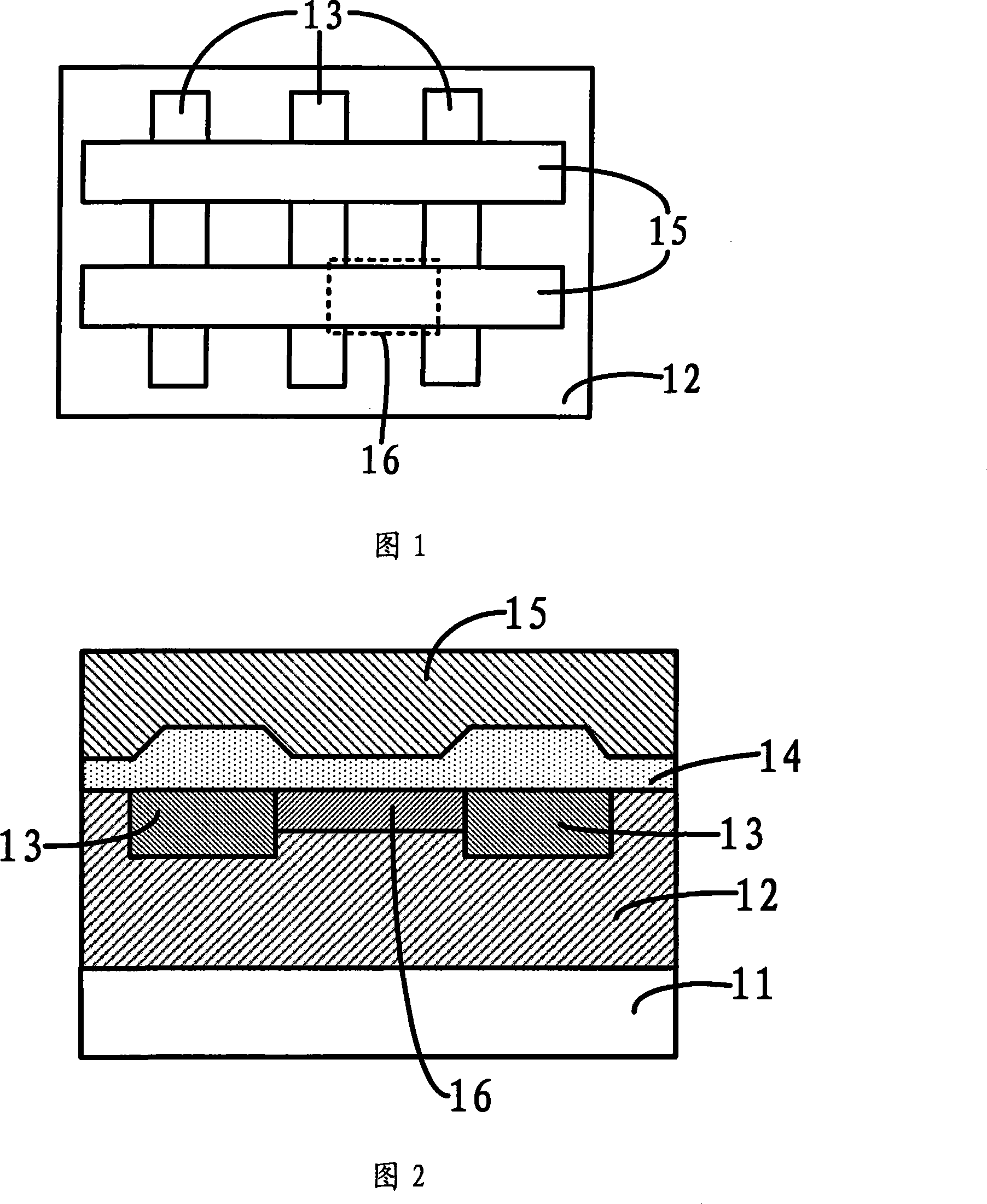
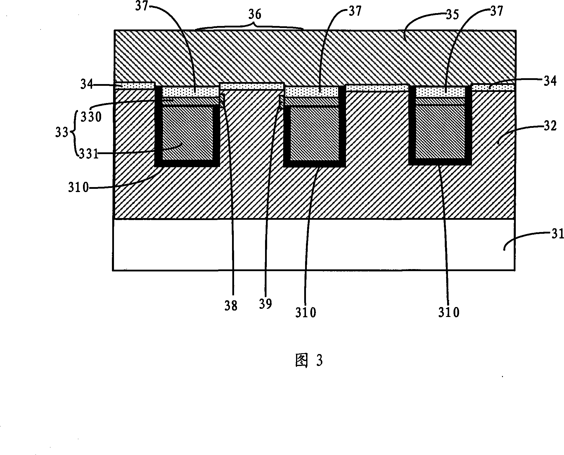
[0028] Referring to FIG. 3, it shows a cross-sectional view of the first embodiment of the mask ROM of the present invention. As shown in the figure, the mask ROM is fabricated in a conductive well 32 on a silicon substrate 31, which includes A plurality of bit lines 33 and word lines 35 arranged in parallel, the plurality of word lines 35 are vertically arranged on the bit lines 33 (the arrangement structure can be referred to FIG. 1 ), the mask read-only memory There are a plurality of coding regions 36, the coding regions 36 cover the word line 35 between the bit lines 33 and the local area adjacent to the bit line 33, there is a gate oxide layer 34 between the word line 35 and the silicon substrate 31, the A shallow trench is opened in the conductive well 32 for the bit line 33, and a diffusion barrier layer 310 is deposited on the w...


PUM

PropertyMeasurementUnit
Thickness rangeaaaaaaaaaa
Thicknessaaaaaaaaaa
Thicknessaaaaaaaaaa

Abstract

The invention provides a MROM and a method for manufacturing the same, wherein the MROM comprises a plurality of bit lines and word lines, and also has a plurality of word lines covering between every two bit lines and a coding region of adjacent local regions of two bit lines. The prior art adopts the buried layer source electrode and drain electrode of a transistor as the bit line of a MROM; however, the MROM can not scale down and the reading-out speed of the MROM slows down when minimum feature size contracts continuously. The MROM provided by the invention is made inside the conductive well which is arranged on a silicon substrate and is provided with a shallow ditch groove arranged according to the bit lines, wherein a diffusion barrier layer is deposited on the wall of the shallow ditch groove; the bit lines, which are arranged inside the shallow ditch groove, are separated from the word lines through the isolation oxidation layer arranged inside the shallow ditch groove; moreover, the bit lines comprises an upper layer of heavy doping multicrystal silicon and a lower layer of heavy doping multicrystal silicon which are stacked; the conductive well is in direct contact with the isolation oxidation layer of a coding region and the upper layer of heavy doping multicrystal silicon; moreover, the contact area of the conductive well with the upper layer of heavy doping multicrystal silicon is provided with a source heavy doping region and a drain heavy doping region. The invention is convenient for scalingdown of the MROM and can increase reading-out speed.

Description

technical field [0001] The invention relates to memory technology, in particular to a mask read-only memory and a manufacturing method thereof. Background technique [0002] Mask Read Only Memory (MROM for short) is one of the common types of non-volatile (No-Volatile) memory, which is widely used in electronic products. Referring to FIG. 1 and FIG. 2 , they are respectively a top view and a cross-sectional view of a mask ROM commonly used in the industry at present. As shown in the figure, the mask ROM is fabricated in a conductive well 12 of a silicon substrate 11, which includes respectively A plurality of bit lines 13 and word lines 15 arranged in parallel, the plurality of word lines 15 are vertically arranged on the plurality of bit lines 13, and the plurality of bit lines 13 and word lines 15 are separated by a gate oxide layer 14 Open, the mask read-only memory also has a plurality of coding regions 16, the coding regions 16 are located in the conductive well 12 and...

Claims


Application Information

Patent Timeline
IPC IPC(8): H01L27/112H01L21/8246G11C17/12
Inventor 高文玉江柳王庆东
Owner GRACE SEMICON MFG CORP
Why Eureka
Try Eureka