
Device and method for focusing and leveling based on microlens array

A micro-lens array, focusing and leveling technology, applied in the field of optical measurement, can solve the problems of difficult to improve single-point measurement accuracy, reduce system measurement accuracy, and high requirements for light source stability, so as to improve measurement accuracy and overall system adaptability. , The effect of reducing the requirements of light source stability and reducing the difficulty of optical design

Inactive Publication Date: 2008-06-18
BEIJING INSTITUTE OF TECHNOLOGYGY
View PDF2 Cites 40 Cited by
  • Summary
  • Abstract
  • Description
  • Claims
  • Application Information

AI Technical Summary

Problems solved by technology

This technology has the following shortcomings: First, the multi-slit array is imaged on the same surface through the same imaging system, and the imaging problem of large field of view needs to be considered in the optical design, which increases the difficulty of optical design; secondly, the single The scanning mirror scans all the light points uniformly through the receiving slit array, which makes it difficult to improve the measurement accuracy of a single point, thereby reducing the measurement accuracy of the system; also higher

Method used

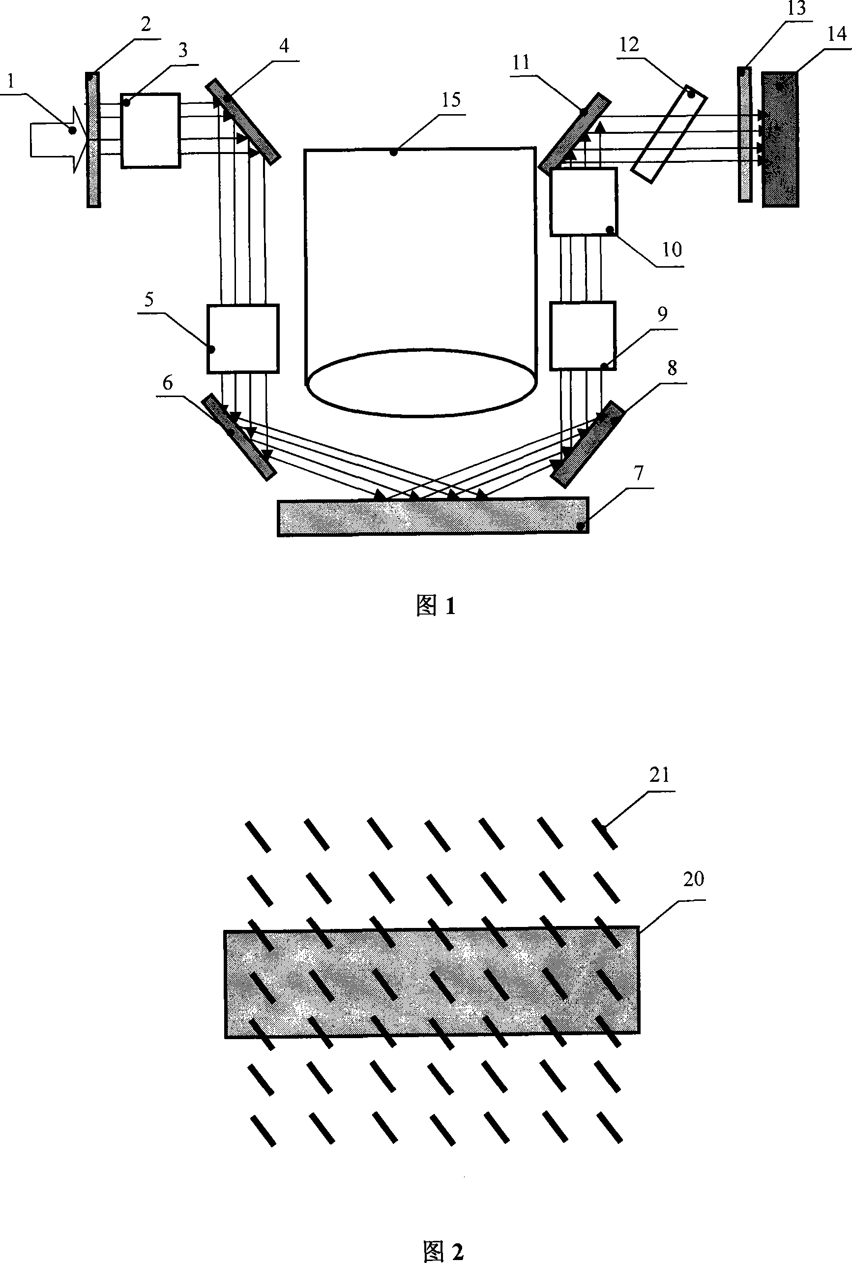

Image

  • Device and method for focusing and leveling based on microlens array
  • Device and method for focusing and leveling based on microlens array
  • Device and method for focusing and leveling based on microlens array

Examples


Embodiment Construction

[0036] The present invention will be further explained below in conjunction with the drawings.

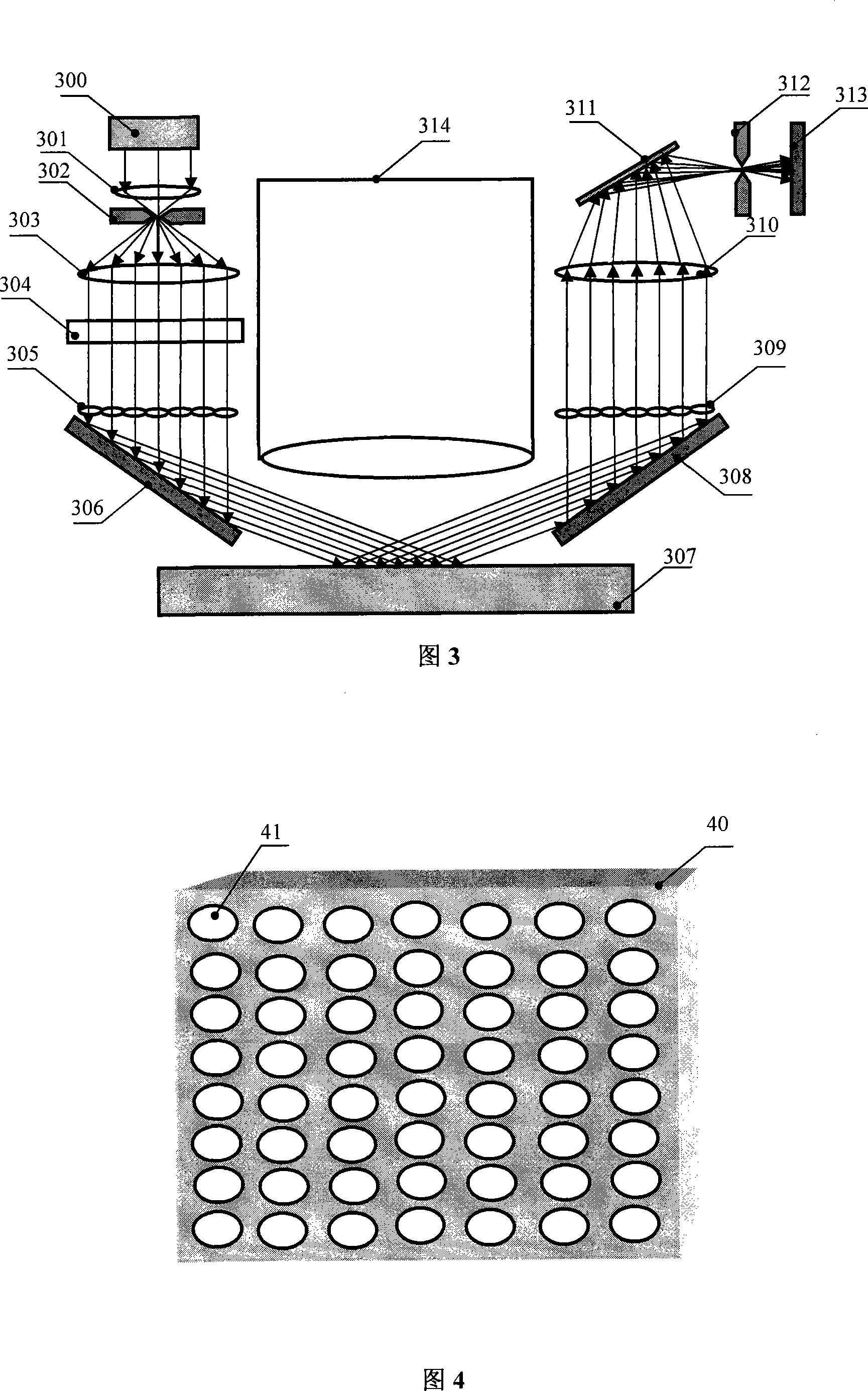
[0037] As shown in FIG. 3, it is a schematic diagram of the structure of the focusing and leveling system of the lithography machine of the present invention. The optical system of the focusing and leveling device of the present invention includes two large modules, namely a transmitting module and a receiving module.

[0038] Hereinafter, each component module of the optical system of the present invention will be described one by one with reference to FIG. 3.

[0039] The light source 300 is reshaped, focused by the focusing lens 301 and incident on the pinhole filter 302, and then expanded by the beam expander lens 303. The beam-expanded parallel light is controlled by the optimizing entrance pupil device 304 to control the amount of light passing. After 304, the micro lens array 305 is used to align the corresponding parallel light beams, and the light passes through the micro lens...


PUM


Abstract

The invention discloses a method and a device based on focusing and leveling of a lenticule array and belongs to the technical field of opto-electrical detection. The invention comprises an emitting part and a receiving part, wherein, the emitting part comprises a light source, a focusing lens, a pinhole filter, a beam expanding lens, an optimal entrance pupil device, a lenticule array and a steering mirror; the receiving part comprises a steering mirror, a lenticule array, a focusing lens, a scan mirror of a micro-opto-electro-mechanical-system (OMEMS), a pinhole filter and a detector. The invention adopts the optimal entrance pupil device to control light entrance quantity and then improve measuring light spot, or the quantity of the imaging point can be controlled by the state of a switch to adapt to different exposure viewing field; the invention adopts the lenticule array to replace a slit array; the scan mirror of the micro-opto-electro-mechanical-system (OMEMS) is adopted to replace the single lens scan; the difference receiving method is adopted and then the requirement for stability of the light source is decreased and higher measuring accuracy can be acquired.

Description

Technical field [0001] The invention relates to a focusing and leveling detection method and device used in a projection lithography system. Its main function is to perform high-precision detection of the distance between the surface of the exposed silicon wafer and the projection objective lens and the two-dimensional inclination angle of the silicon wafer , In particular, a focusing and leveling sensor with simultaneous measurement of multiple points, which belongs to the field of optical measurement. Background technique [0002] In the projection lithography system, the silicon wafer focusing and leveling measurement system is used in the lithography machine to measure the height and rotation angle (Z, θ) of the silicon wafer surface relative to the projection objective lens. X And θ Y ), forming a feedback system with three vertical actuators of the workpiece table, real-time control of the vertical position of the silicon wafer, to ensure that the current field of the silic...

Claims


Application Information

Patent Timeline
IPC IPC(8): G03F7/20G03F9/00
Inventor 匡翠方李艳秋刘丽辉
Owner BEIJING INSTITUTE OF TECHNOLOGYGY
Learn More