

Drive voltage control device
A technology for driving voltage and control devices, applied to instruments, static indicators, etc., can solve problems such as difficult to eliminate the limitation of speed limit
- Summary
- Abstract
- Description
- Claims
- Application Information
AI Technical Summary
Problems solved by technology
Method used
Image

Examples
Embodiment 1
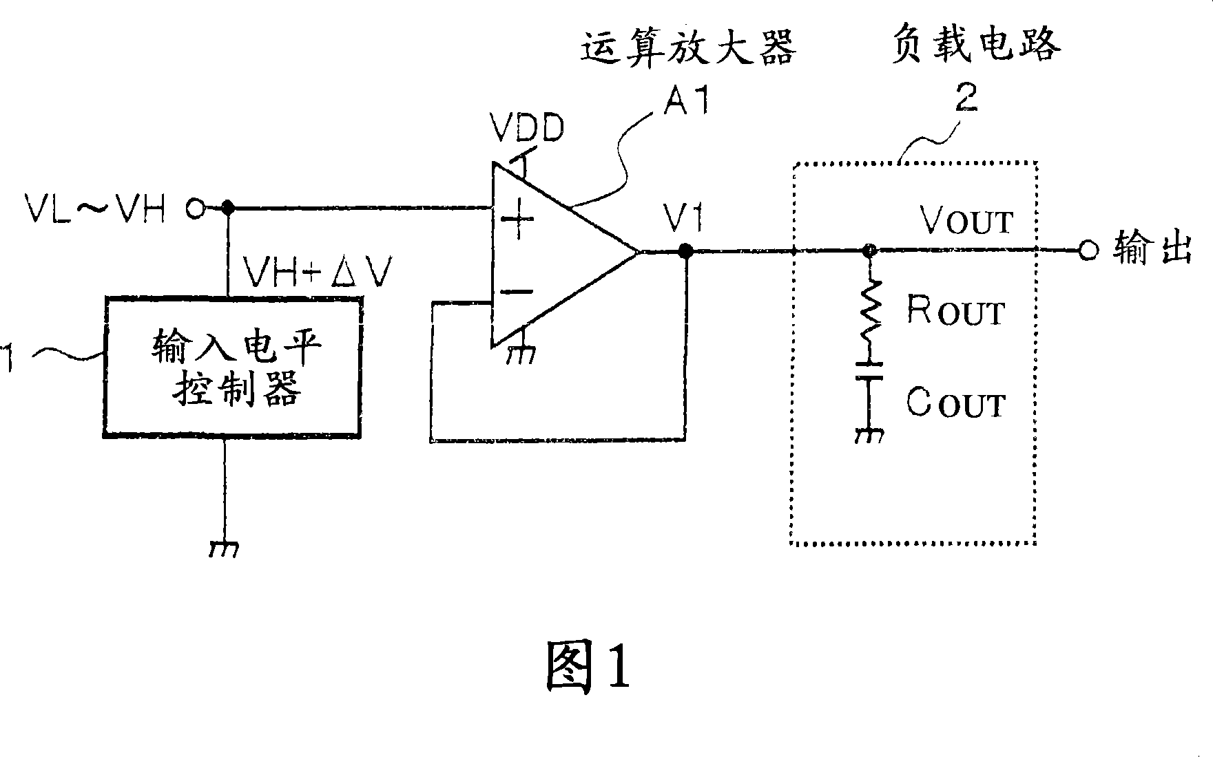
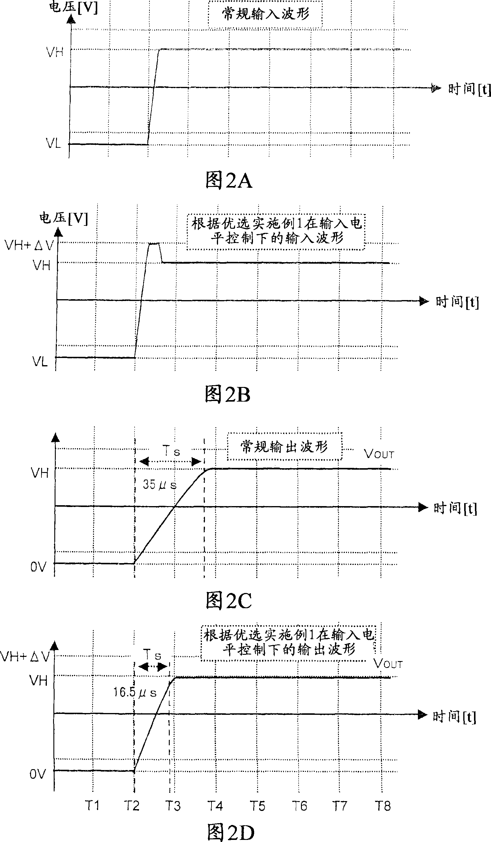
[0209] FIG. 1 is a circuit diagram showing the structure of a driving voltage control device for a liquid crystal panel according to a preferred embodiment 1 of the present invention. In FIG. 1 , A1 denotes an operational amplifier as a suitable example of a buffer, 1 denotes an input level controller, and 2 denotes a load circuit. The output of operational amplifier A1 is fed back to its inverting input (-). The load circuit 2 of the LCD panel includes a load resistor R OUT and load capacitance C OUT , and connect to the output of op amp A1. The load circuit 2 is represented in the form of an equivalent circuit. The input level controller 1 is interposed between the non-inverting input terminal (+) of the operational amplifier A1 and ground, and controls the level of the voltage applied to the non-inverting input terminal (+) of the operational amplifier A1. The output terminal OUT outputs a high-level target driving voltage VH having a high voltage and a low-level target...
Embodiment 2
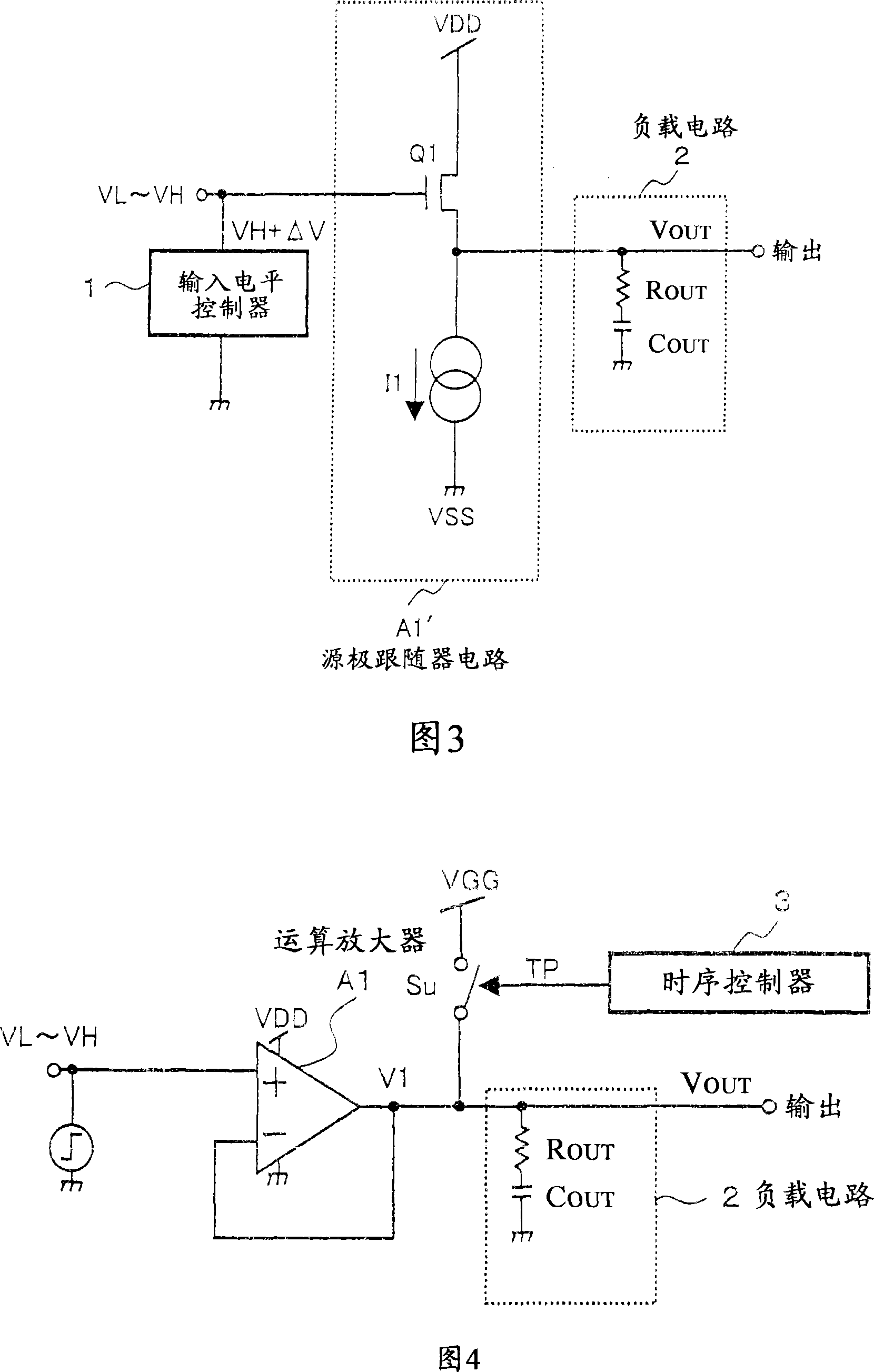
[0237] 4 is a circuit diagram showing the structure of a driving voltage control device for a liquid crystal panel according to a preferred embodiment 2 of the present invention. The input signal is input to the non-inverting input (+) of operational amplifier A1. The output terminal of the operational amplifier A1 is connected to the LCD panel including the load resistor R OUT and load capacitance C OUT The load circuit 2. VGG represents a boosted voltage having a potential higher than that of the power supply voltage VDD of the operational amplifier A1. The output terminal of the operational amplifier A1 is connected to the power supply of the boost VGG through the boost control switch Su. The timing controller 3 turns on and off the boost control switch Su based on the control signal TP.
[0238] 5B and 5C illustrate the above operation. FIG. 5A shows a load driving voltage according to a conventional technique. The timing controller 3 turns on the boost control switc...
Embodiment 3
[0259] 8 is a circuit diagram showing the structure of a driving voltage control device for a liquid crystal panel according to a preferred embodiment 3 of the present invention. Components that are the same as previously described are provided with the same reference numerals. The high-level side DC target driving voltage VH of the input signal determined by the pixel data of the liquid crystal display and the boosted voltage VHH higher than the high-level side target driving voltage VH are selectively input to the operational amplifier A1 through the input selection switch Si Non-inverting input (+). The smoothing capacitor CC is interposed between the output terminal of the operational amplifier A1 and the ground, and the output control switch So is interposed between the smoothing capacitor CC and the load circuit of the liquid crystal panel. The boosted voltage VHH is higher than the high-level side target drive voltage VH, and the difference ΔVHH=(VHH−VH) between the tw...
PUM
 Abstract
Description
Claims
Application Information