Semiconductor memory and method for forming same

A semiconductor and memory technology, applied in the field of semiconductor memory and its formation, can solve the problems of poor integration between semiconductor memory circuits and logic circuits, and difficulty in realizing high-density storage, and achieve high integration and high-density storage functions.

Active Publication Date: 2008-06-18
SEMICON MFG INT (SHANGHAI) CORP +1
View PDF0 Cites 14 Cited by
  • Summary
  • Abstract
  • Description
  • Claims
  • Application Information

AI Technical Summary

Problems solved by technology

[0007] The problem solved by the present invention is that the semiconductor storage circuit and the logic circuit in the prior art are poorly integrated, and it is difficult to realize high-density storage

Method used


Image

  • Semiconductor memory and method for forming same
  • Semiconductor memory and method for forming same
  • Semiconductor memory and method for forming same

Examples


Embodiment Construction

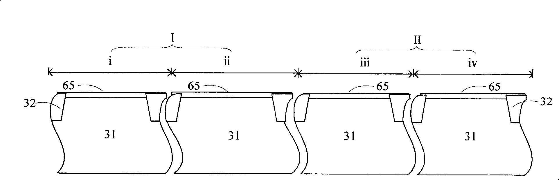
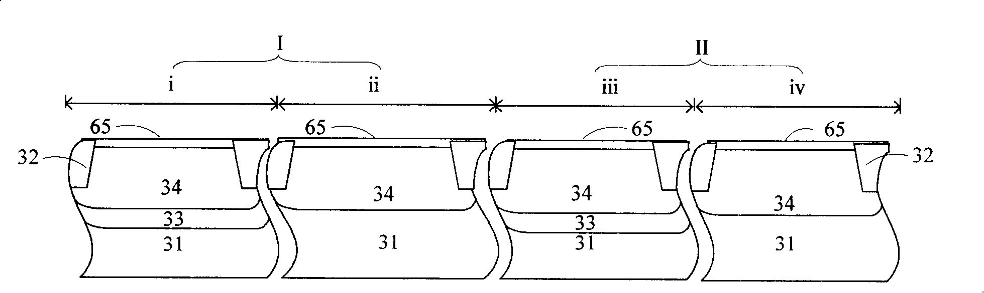
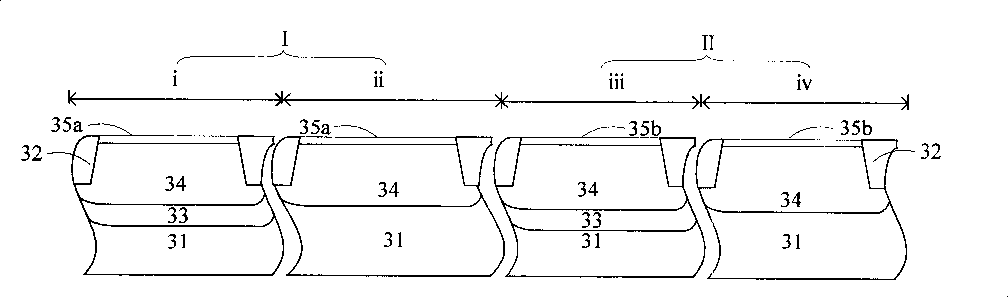
[0044] The essence of the invention is a method for integrating a semiconductor memory and a logic CMOS circuit. The semiconductor memory is formed by forming a charge trap in a gate dielectric layer of a MOS transistor. The invention provides a method for forming a semiconductor memory and its structure: for a MOS transistor whose gate dielectric layer is made of silicon oxide, silicon nitride or a combination thereof, ionization is carried out to the gate dielectric layer of the storage circuit region on the semiconductor substrate Implantation forms charge traps so as to have the ability to store charges, and at the same time, ion implantation is not performed in the logic circuit area on the semiconductor substrate. The present invention provides a semiconductor with a core circuit area, which is the I region, and an input and output circuit region, which is the II region. Substrate, and then by ion implantation in the core storage circuit area of ​​the I region, that is, t...


PUM


Abstract

The forming method of a semiconductor memory comprises a semiconductor substrate which comprises an IA area and an IB area, and gate dielectric layers and gates are formed on the semiconductor substrate sequentially, the gate dielectric layer of the IA area is an electric charge trap area, while the gate dielectric layer of the IB area is a non-electric charge trap area, an active power extension area or a leaking extension area is formed on the IA area and the IB area of the semiconductor substrate, a source electrode or a drain electrode is formed on the IA area and the IB area of the semiconductor, correspondingly the invention also provides a semiconductor memory and a semiconductor device and the forming method thereof; the semiconductor memory formed by the invention has the function of double bytes storage so as to realize the high-density storage function, at the same time, the logic circuit and the storage circuit formed by adopting the invention can be compatible with each other.

Description

technical field [0001] The invention relates to the technical field of semiconductors, in particular to a semiconductor memory and a forming method thereof. Background technique [0002] A non-volatile semiconductor memory device, such as a flash memory device, is capable of storing data when the semiconductor device is powered off. The memory cells of the flash memory device may include electrically isolated floating gates, respectively on the first and second sides of the floating gates in the substrate. and a control gate configured to control the floating gate. Typically, the threshold voltage of a flash memory cell depends on the amount of charge stored in the floating gate. Data stored in the flash memory cells can be detected by sensing the amount of change in the cell current of the flash memory cells caused by the threshold voltage difference. [0003] The single-chip system (System-on-Chip, SoC) system generated by the integration of the flash semiconductor memor...

Claims


Application Information

Patent Timeline
Patent Type & Authority Applications(China)
IPC IPC(8): H01L21/8247H01L21/8234H01L21/8238H01L27/115H01L27/088H01L27/092
CPCB82Y10/00H01L27/11573H01L27/105H01L27/11568H10B43/40H10B43/30
Inventor 季明华
Owner SEMICON MFG INT (SHANGHAI) CORP
Why Eureka
Try Eureka