

Method for controlling semiconductor silicon dies etching technique
A semiconductor and silicon wafer technology, applied in the field of feedback control of semiconductor silicon wafer etching process, can solve the problems of complex process, large human resources and expenses, and achieve the effects of low cost, complex saving and precise control
- Summary
- Abstract
- Description
- Claims
- Application Information
AI Technical Summary
Problems solved by technology
Method used
Image

Examples
Embodiment Construction
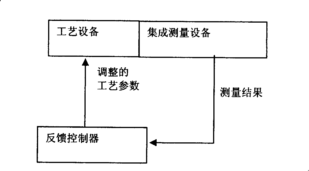
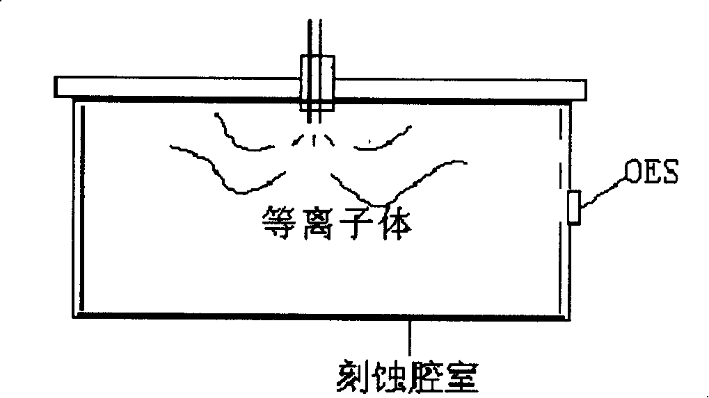
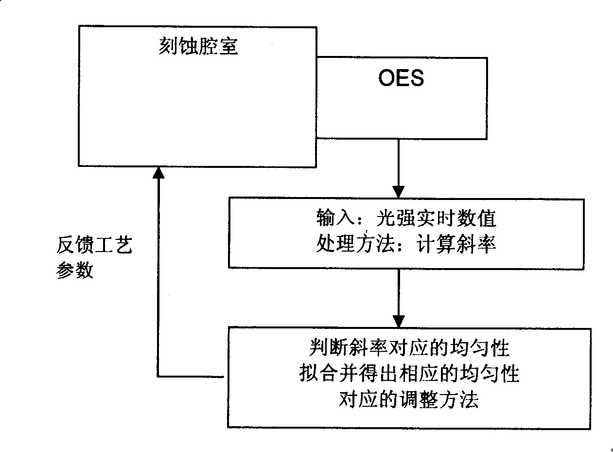
[0029] The feedback control method of semiconductor silicon chip etching process of the present invention, as figure 2 As shown, the silicon wafer etching process is performed in an etching chamber, and an OES (Optical Scattering Spectrometer) is installed on the etching chamber to control the end point of the etching process.
[0030] The integrated OES is usually used to control the etching end point on the etching equipment. When etching from one film of a silicon wafer to another film, since the etching process is required to have different etching rates when etching different film layers, a certain selectivity ratio is required. For the next layer of film, the etching process can be judged from the emission spectrum intensity of the etching product by using OES detection, so as to stop etching, change the process parameters and then etch the next layer of film. Therefore, OES equipment is the necessary hardware for etching equipment, and it is mainly used for etching en...
PUM
 Abstract
Description
Claims
Application Information