Solder tappet structure and its making method

A solder bump and solder technology, applied in semiconductor/solid-state device manufacturing, electrical components, electrical solid-state devices, etc., can solve problems such as chip failure, weakening the bonding force between bonding pads and solder bumps, and affecting the long-term reliability of wiring, etc. Achieve the effect of improving reliability, reducing the degree of undercutting, and being less prone to damage

Active Publication Date: 2010-12-08
TAIWAN SEMICON MFG CO LTD
View PDF5 Cites 0 Cited by
  • Summary
  • Abstract
  • Description
  • Claims
  • Application Information

AI Technical Summary

Problems solved by technology

Although the undercut is an inevitable result of the etching step, the undercut can affect the long-term reliability of the wiring, because the undercut will weaken the bonding force between the bonding pad and the solder bump, and reduce the integrity of the solder bump structure. cause the chip to fail prematurely

Method used


Image

  • Solder tappet structure and its making method
  • Solder tappet structure and its making method
  • Solder tappet structure and its making method

Examples


Embodiment Construction

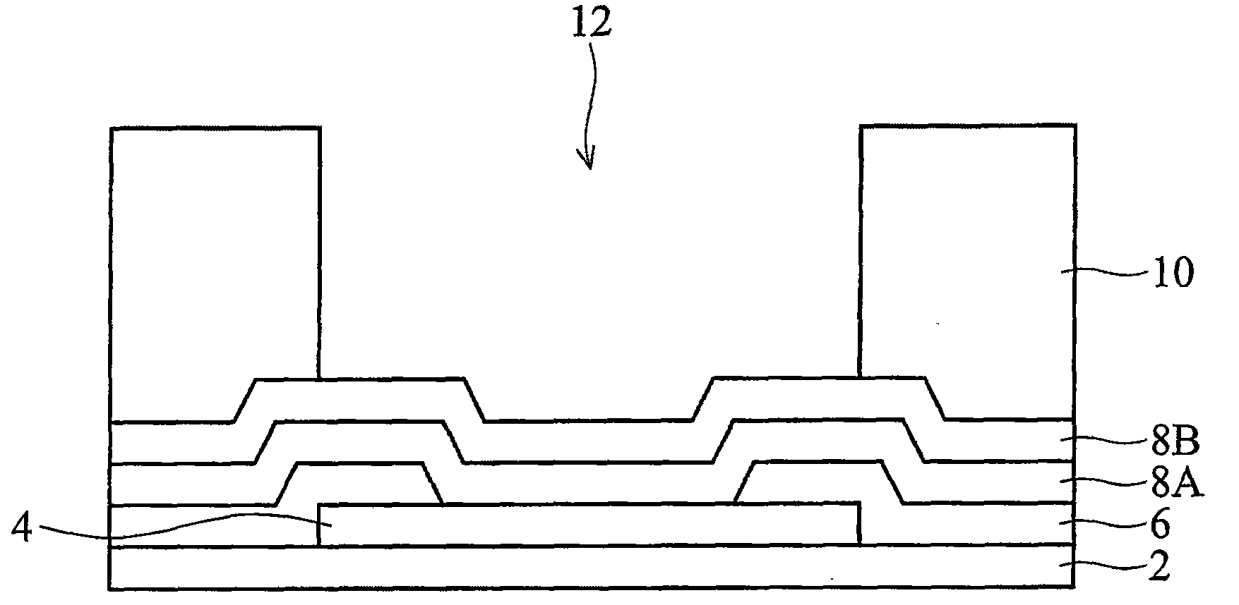
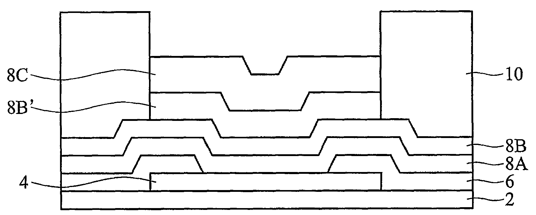
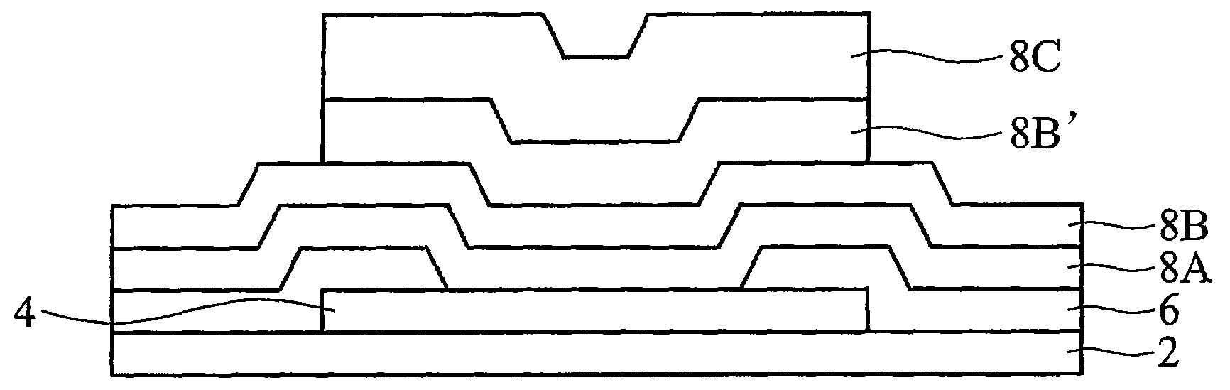
[0031] Please refer to Figure 2A , which shows a cross-sectional view of a solder bump structure fabricated according to an embodiment of the present invention, wherein the bonding pad 4 is disposed on the semiconductor substrate 2 . The bonding pad 4 has a patterned protection layer 6 , and the protection layer 6 exposes a part of the bonding pad 4 . Bonding pads or contact pads are usually electrically connected to the chip through multilayer metal interconnection. The bonding pad 4 can be formed by conventional chemical vapor deposition (CVD, chemical vapor deposition), and the material is copper, aluminum, or other conductive metals, for example. After the bonding pads 4 are formed, a protection layer 6 is deposited on the surface of the bonding pads 4 as protection and electrical isolation. The protective layer 6 can isolate the surface of the chip and protect the chip from moisture or pollutants, and from mechanical damage during assembly. The protective layer 6 can ...


PUM


Abstract

A method of manufacturing a solder bump structure on a semiconductor device is provided. In one embodiment, a semiconductor substrate is provided having a bonding pad and a passivation layer formed thereabove, the passivation layer having an opening therein exposing a portion of the bonding pad. A first under bump metallization (UBM) layer is formed over the bonding pad and the passivation layer.A mask layer is placed over the first UBM layer, the mask layer having an opening therein exposing a portion of the first UBM layer. The mask layer is thereafter etched to create a recess at the edges between the first UBM layer and the mask layer. A second UBM layer is deposited in the opening of the mask layer, the second UBM layer filling the recess and a portion of the opening of the mask layer.

Description

technical field [0001] The present invention relates to the fabrication of semiconductor elements, and in particular to a method of fabricating a solder bump structure on a semiconductor element. Background technique [0002] Under bump metallization (UBM, under bump metallization) has been widely used in semiconductor manufacturing processes. The semiconductor manufacturing process generally includes steps such as thin film deposition, patterning, doping, and heat treatment on the semiconductor wafer. After the semiconductor element is manufactured, it also includes testing, packaging and assembling the semiconductor integrated circuit chip (IC chip) on the wafer. Flip chip packaging is an advanced semiconductor packaging technology, which is characterized in that after the chip is turned upside down, the conductive bumps or bonding pads on the chip are directly connected to external components (such as substrates) ) connection, so that conductive contact can be achieved....

Claims


Application Information

Patent Timeline
Patent Type & Authority Patents(China)
IPC IPC(8): H01L21/60
CPCH01L2924/14H01L2924/014H01L2924/01022H01L2224/11472H01L2224/11462H01L2224/11831H01L2924/01006H01L2924/01015H01L2924/01078H01L2924/00013H01L2924/01018H01L2924/01033H01L24/11H01L2224/1147H01L2924/01075H01L2924/01029H01L2924/01013H01L24/12H01L2224/131H01L2924/01082H01L2224/05027H01L2224/05022H01L2224/0508H01L2224/05001H01L2224/05572H01L2224/05124H01L2224/05147H01L2224/05155H01L2224/05166H01L2224/056H01L24/13H01L24/05H01L24/03
Inventor 张碧兰游秀美黄志恭邱颂盛
Owner TAIWAN SEMICON MFG CO LTD
Why Eureka
Try Eureka